Dopant Activation
Dopant activation is the step that makes dopant atoms introduced by ion implantation electrically active. Right after implantation, most atoms of arsenic, phosphorus or boron sit between lattice sites or in damaged clusters and supply no carriers. An anneal repairs the crystal and moves them onto substitutional lattice sites, where they donate electrons or accept them to create holes.
Also called: activation anneal, electrical activation
Diagram
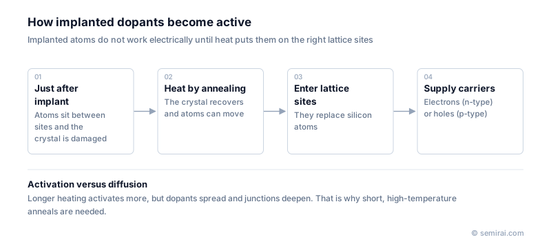
What happens during the anneal
Implantation displaces silicon atoms, and at high doses it turns the surface layer amorphous. When the wafer is heated, an amorphous layer regrows epitaxially from the crystal below, incorporating dopants onto lattice sites as it goes; damaged but still crystalline regions recover by recombining vacancies and interstitials. The fraction of implanted atoms that ends up active is the activation ratio.
Activation is never unlimited. Each dopant has a solid solubility that rises with temperature, and atoms beyond it stay in inactive clusters or precipitates. Boron in particular forms clusters with silicon interstitials. Dopants activated above the equilibrium limit can also deactivate again if later steps heat the wafer for long.
Activation versus diffusion
Higher temperature activates more dopant, but it also makes the dopant diffuse and deepens the junction, and implant damage briefly speeds diffusion further, an effect called transient enhanced diffusion. The history of annealing is a steady shortening of time at high temperature: furnace anneals of tens of minutes, then rapid thermal annealing and spike anneals of about a second, then flash lamp anneals of milliseconds and laser anneals ranging from scanned millisecond heating that stays below the melting point to nanosecond pulses that briefly melt the surface. The shorter the anneal, the more the dopant can be activated with little movement, and melt anneals can even exceed the equilibrium solubility.
At advanced nodes, much source/drain doping is done during epitaxial growth instead, for example boron in SiGe or phosphorus in silicon, which places dopants on lattice sites as the crystal grows and reduces the need for heavy implants.
How activation is measured
Sheet resistance measured with a four-point probe after the anneal is the everyday check, often mapped across the wafer. Secondary ion mass spectrometry (SIMS) gives the total dopant profile, while spreading resistance profiling, Hall measurements and capacitance-voltage methods give the active carrier profile; comparing them shows how much is active and where.
Japanese companies involved
- Ushio developed flash lamp technology for activating ion-implanted silicon with millisecond heating.
- Kokusai Electric makes vertical batch furnaces used for longer, lower-temperature anneals and other thermal steps.
- Ushio · Light sources and exposure systems for packaging
- Kokusai Electric · Batch deposition, diffusion and ALD equipment
FAQ
Why is activation not 100%?
Above the solid solubility limit at the anneal temperature, extra dopant atoms cannot all fit on lattice sites and remain in clusters or precipitates. Residual implant damage also traps some atoms. Very high concentrations, as in source/drain contacts, are therefore partly inactive unless very short or melt anneals are used.
Can active dopants become inactive again?
Yes. Concentrations above equilibrium solubility, reached with very short anneals, are metastable. If later process steps hold the wafer at moderate temperatures for long enough, dopants can cluster or precipitate and sheet resistance rises. This is one reason the thermal budget after activation is kept low.
Comparisons
Related pages
Sources
Ion implantation and thermal processing terms
Last updated: November 2, 2026