Cryogenic Ion Implantation
Cryogenic ion implantation is ion implantation performed with the wafer cooled to around −100 °C or lower. Cooling suppresses the movement of defects during the implant, so the damaged layer becomes more cleanly amorphous and fewer defects remain after annealing. This helps reduce leakage current and transient enhanced diffusion.
Also called: cryo implant, low-temperature implantation
Diagram
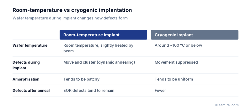
Why cooling changes the damage
In a normal implant the wafer is at room temperature or slightly warmer from beam heating. Implanted ions knock silicon atoms out of place, and at room temperature some of this damage moves, recombines or clusters even while the implant continues. This is called dynamic annealing, and it leaves a patchy mix of damaged crystal and amorphous pockets.
Cooling the wafer freezes this movement, so the same dose produces a more uniform amorphous layer. When it regrows during annealing, fewer end-of-range (EOR) defects remain below the original amorphous/crystal boundary. Fewer leftover interstitials also means less transient enhanced diffusion (TED).
Applications and practical issues
Thin fins in FinFETs are hard to regrow cleanly after implantation, and leftover defects can raise resistance and leakage. Cryogenic implantation has been studied and adopted as a way to reduce this damage.
The implanter needs a chuck that keeps the wafer cold throughout the implant, and a way to warm wafers in a dry environment before they leave the vacuum, so that moisture does not condense on them. The time spent cooling and warming lowers throughput, which equipment makers work to minimise.
Japanese companies involved
- Sumitomo Heavy Industries Material Solutions (formerly SMIT) and Nissin Ion Equipment make ion implanters, where wafer temperature during implantation is one of the parameters engineers can control.
- Nissin Ion Equipment · Ion implanters
- Sumitomo Heavy Industries Material Solutions (formerly SMIT) · Ion implanters
FAQ
Why does a cleaner amorphous layer mean fewer defects?
A uniform amorphous layer regrows by solid phase epitaxy with a flat, well-defined front, leaving few defects behind. A patchy layer regrows unevenly, and the clusters formed during implantation can grow into stable dislocation loops.
Is cryogenic implantation used for every implant?
No. It costs throughput and needs extra hardware, so it is used where implant damage matters most, such as shallow junctions and narrow 3D structures. Many implants still run at room temperature, and some are deliberately run hot to avoid amorphisation.
Related pages
Sources
Ion implantation and thermal processing terms
Last updated: November 2, 2026