Probe Mark (Scrub Mark)
A probe mark, or scrub mark, is the scratch-like mark left on a chip's bond pad when a probe card needle is pressed onto it during wafer test. The needle slides slightly sideways, or scrubs, to break through the thin oxide on the pad surface and contact the metal below, so a small mark is always left.
Also called: scrub mark, probe scrub
Diagram
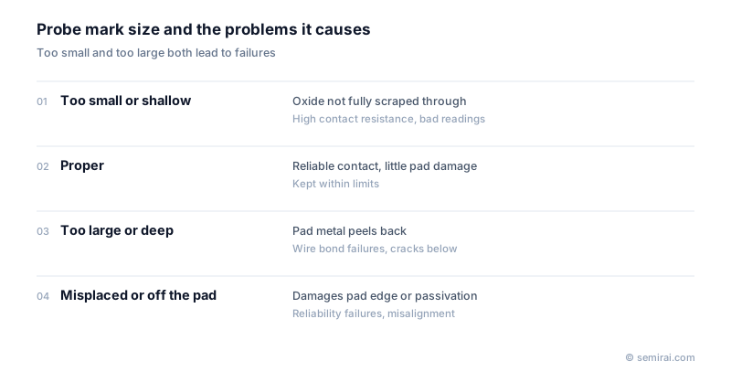
Why size matters
A mark that is too small or too shallow means the oxide was not fully broken. Contact resistance is high and the measurement is unreliable, which can cause good dies to be rejected.
A mark that is too large or too deep can peel back or thin the pad metal. The ball in later wire bonding then does not adhere properly, and cracks can form in the insulating layers or circuits under the pad. A mark that runs off the edge of the pad can damage the passivation layer and cause reliability failures.
Inspection and control
After wafer test, the position, size and depth of probe marks are inspected optically and checked against limits. A shift in mark position points to a problem in prober alignment or in the condition of the needle tips, so the inspection also works as a health check of the probing set-up.
Pads are getting smaller, and more devices are probed on fragile structures such as copper pillars and micro-bumps. Probe cards and probers are therefore designed to apply less force and leave smaller marks while still making reliable contact.
Japanese companies involved
- Micronics Japan makes probe cards, whose needle design and contact force determine the size of the scrub mark.
- Tokyo Seimitsu (ACCRETECH) makes wafer probers that control the overdrive and alignment that set where and how deeply the needles land.
- Micronics Japan · Probe cards
- Tokyo Seimitsu (ACCRETECH) · Wafer probers, dicing and grinding machines, metrology
FAQ
Why do probe marks form at all?
Aluminium and other pad metals carry a thin native oxide that does not conduct well. The probe must scrape through it to reach clean metal, so it is pushed down past first contact (overdrive) and slides a short distance. That scrubbing motion leaves the visible mark.
How do probe marks affect wire bonding?
If a mark is large or deep, the pad surface is rough or thinned where the ball is placed. Bond strength drops and the wire can lift. Engineers therefore limit mark area relative to pad area and, on small pads, sometimes separate the probing area from the bonding area.
Related pages
Sources
Last updated: November 13, 2026