Wafer Test (Wafer Sort)
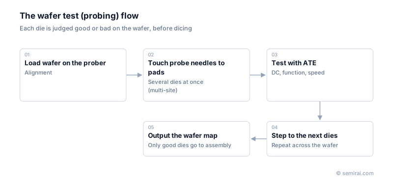
Wafer test, also called wafer sort or probing, is the electrical test of each die while it is still part of the wafer, before dicing. A wafer prober positions the wafer, a probe card makes contact with the die pads, and automated test equipment runs the tests, so that only good dies go on to assembly.
Also called: wafer sort, wafer probing, circuit probe (CP), probe test
Diagram
Why test at wafer level
Packaging, assembly and final test cost money for every die that enters them. Removing defective dies first means that money is spent only on good ones. For multi-chip packages, chiplets and stacked memory the stakes are higher, because one bad die can scrap a whole module containing several expensive good ones; wafer test is the main tool for delivering known good dies (KGD).
Wafer test also feeds back to the fab. Dies that fail are recorded on a wafer map, and the pattern of failures across the wafer, such as a ring at the edge or a cluster, often points to the process step that caused them. Test structures in the scribe lines are measured to monitor transistor and interconnect parameters.
How probing works
The prober loads a wafer onto a chuck, aligns it with cameras and raises it so that the probe needles touch the pads, slightly overdriving them to break through surface oxide. The tester runs the program; then the prober steps to the next site. Probe cards that contact several or many dies per touchdown raise throughput, and memory probe cards can contact a large part of the wafer at once.
The chuck can heat or cool the wafer to test at the temperatures the product must guarantee. Results are kept as electronic maps rather than the ink dots used in the past.
Limits of wafer test
Needles leave probe marks on the pads, which must stay small enough not to harm later wire bonding or bumping. Thin needles also limit current and high-frequency performance, so some speed and power tests are left to final test. Defects created by assembly cannot be seen at this stage.
Japanese companies involved
- Tokyo Seimitsu (ACCRETECH) and Tokyo Electron make wafer probers, Micronics Japan makes probe cards, and Advantest makes the testers used at wafer sort.
- Tokyo Electron (TEL) · Coat/develop, etch and deposition equipment
- Advantest · Automated test equipment (ATE) for SoC and memory
- Tokyo Seimitsu (ACCRETECH) · Wafer probers, dicing and grinding machines, metrology
- Micronics Japan · Probe cards
FAQ
What happens to dies that fail wafer test?
They are marked as failures on the electronic wafer map, which the assembly line reads when it picks dies after dicing, so failed dies are simply left behind. Some memory dies with failing cells are instead repaired by switching in spare rows or columns.
What is a touchdown?
A touchdown is one contact of the probe card with the wafer. The number of touchdowns needed to cover the wafer, and the time per touchdown, set the throughput, so multi-die probe cards are used whenever the tester has enough channels.
What is a parametric test at wafer level?
It measures simple structures such as single transistors, resistors and capacitors placed in the scribe lines, rather than the product circuit. It checks that the process ran within limits and is often done before the full functional wafer test.
Comparisons
Related pages
Sources
Last updated: November 13, 2026