Failure Analysis (FA)
Failure analysis (FA) is the work of examining failed devices to find the physical root cause and decide whether design, wafer processing or assembly was at fault. Testing answers whether a chip is bad; FA answers why it went bad, and it supports both yield improvement and prevention of repeat field failures.
Also called: FA, physical failure analysis, fault isolation
Diagram
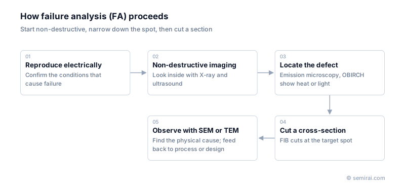
From non-destructive to destructive
The rule is to move from non-destructive to destructive methods, because each destructive step removes evidence. Electrical measurements first classify the symptom as an open, short, leakage or functional failure and confirm that it can be reproduced. Scanning acoustic microscopy (SAT) and X-ray then show delamination, voids and deformed wires inside the package without opening it. If the cause is still unknown, the package is opened (decapsulated) to expose the die.
Once the defect has been located, physical analysis begins. A focused ion beam (FIB) cuts a cross-section at the exact spot, and scanning or transmission electron microscopes (SEM, TEM) image the structure. Energy-dispersive X-ray spectroscopy (EDX) or secondary ion mass spectrometry (SIMS) identifies the elements present. This is where voids in wiring, ruptured gate oxide, metal contamination or trapped particles finally become visible.
Fault isolation: finding the spot
Locating a defect a few hundred nanometres across among billions of transistors is the hardest step. OBIRCH (optical beam induced resistance change) scans a laser over the chip and detects changes in resistance caused by local heating. Emission microscopy captures the faint light given off by abnormal current. On the logic side, scan diagnosis uses test results and scan-chain information to narrow down suspect nets and cells.
FA results always go back into production. A defect traced to a particular tool leads to maintenance or part replacement; a design cause is fixed in the next revision. For field returns, customers expect a report and corrective action, so FA is closely tied to the quality assurance system.
Japanese companies involved
- Hamamatsu Photonics makes emission microscopes and laser-scanning systems used for fault isolation in semiconductor failure analysis.
- JEOL and Hitachi High-Tech make the electron microscopes and FIB systems used to cut and image cross-sections of failing devices.
- Hamamatsu Photonics · Failure analysis, process monitoring and static elimination equipment
- Hitachi High-Tech · CD-SEM metrology, defect inspection and etch systems
- JEOL · Electron beam lithography systems, electron microscopes and surface analysis
FAQ
Why not cut the chip open first?
Because opening or sectioning destroys information. A crack seen in an X-ray image may vanish when the package is opened, and a cross-section through the wrong place ruins the sample. Each step narrows the search so that the destructive cut lands exactly on the defect.
Who performs failure analysis?
Chipmakers have their own FA labs next to their fabs and assembly sites, and independent analysis laboratories also offer FA services. Equipment makers supply the tools, from acoustic microscopes to FIB and TEM systems.
Comparisons
Related pages
- DPPM (Defective Parts Per Million)
- Scanning Electron Microscope (SEM)
- Secondary Ion Mass Spectrometry (SIMS)
- Yield
- Bathtub Curve / FIT Rate
- Chemical Shift (XPS)
- OBIRCH (Optical Beam Induced Resistance Change)
- Focused Ion Beam (FIB)
- Final test equipment
- Advantest 7038 System-Level Test System
- Advantest T2000
- DISCO DIS100
- Tokyo Electron (TEL) Prexa™ SDP
Sources
Last updated: November 1, 2026