Scribe Line
A scribe line is the narrow strip between neighbouring chips on a wafer, reserved for dicing. It is also called a dicing street. Typically about 50-100 µm wide, it is cut through with a blade or laser to separate the wafer into individual chips.
Also called: dicing street, saw street, kerf
Diagram
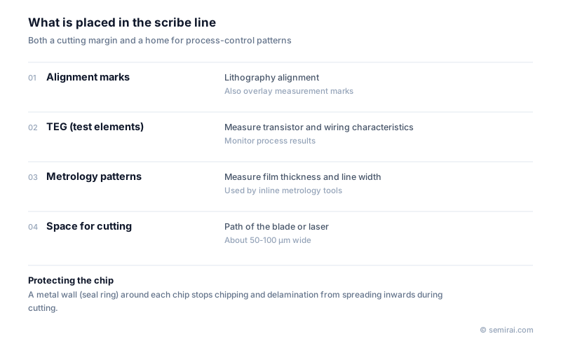
What sits in the scribe line
Besides providing room for the cut, the scribe line holds patterns needed for process control. These include alignment marks for lithography, overlay marks that measure layer-to-layer misalignment, structures for measuring film thickness and line width, and test element groups (TEGs), small test transistors and wiring used to monitor electrical characteristics.
Putting these structures in the scribe line lets the fab monitor every wafer without spending product area, since the strip is destroyed in dicing anyway. Metal patterns left in the street can, however, make cutting harder and cause chipping or burrs, so their layout is agreed between process and assembly engineers.
Width, die count and chip protection
Narrower scribe lines mean more chips per wafer. Blade dicing removes material equal to the blade width, so fabs are moving towards stealth dicing and plasma dicing, which need much less kerf.
Low-k dielectric layers are mechanically weak and can crack or peel. To stop chipping and delamination from spreading into the chip during cutting, a metal wall called a seal ring is built around each chip just inside the scribe line.
Japanese companies involved
- DISCO and Tokyo Seimitsu (ACCRETECH) make dicing saws and laser dicing machines that cut along scribe lines; DISCO developed stealth dicing technology.
- DISCO · Dicing, grinding and polishing equipment
- Tokyo Seimitsu (ACCRETECH) · Wafer probers, dicing and grinding machines, metrology
FAQ
Why put TEGs in the scribe line?
Because that area is cut away anyway, test structures there cost no product area. The fab can measure transistor and wiring characteristics and film properties on every wafer to monitor the process, and the structures disappear when the wafer is diced.
Who benefits most from narrower scribe lines?
Products with very small chips, such as discrete devices, sensors and small microcontrollers. For them the scribe lines take up a large share of the wafer, so narrowing them noticeably increases the number of chips per wafer.
Related pages
Sources
Last updated: November 13, 2026