Low-k Dielectric
A low-k dielectric is an insulating material with a relative permittivity below that of silicon dioxide (k ≈ 3.9), used as the interlayer dielectric between the metal wires of a chip. Lower permittivity reduces the parasitic capacitance between wires, which cuts RC signal delay and switching power.
Also called: low-k, low-permittivity dielectric, ultra-low-k, ULK
Diagram
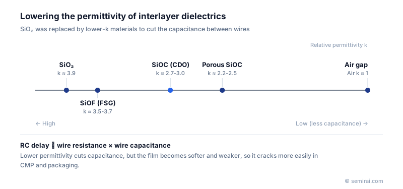
Why interconnects need low-k
As wires shrink, neighbouring lines move closer together and the capacitance between them rises, while thinner wires also have higher resistance. The product, RC delay, increasingly limits chip speed and adds to power consumption. Replacing the insulator with one of lower permittivity attacks the capacitance side of the problem directly.
Materials have moved down in steps: fluorine-doped silicon oxide (FSG, k ≈ 3.5-3.7), carbon-doped oxide (SiOC or CDO, k ≈ 2.7-3.0), and porous SiOC (k ≈ 2.2-2.5), in which tiny pores lower the average permittivity. The ultimate step is an air gap between wires, with k close to 1, which some advanced processes use in selected layers.
Why low-k films are hard to integrate
Lowering k generally means less dense, softer films. Porous low-k has lower mechanical strength, thermal conductivity and chemical resistance than SiO₂, so it can crack or peel under the pressure of chemical mechanical polishing (CMP) or during packaging. Plasma etching and resist ashing can strip carbon from the pore walls and push k back up.
Low-k films are deposited mainly by plasma-enhanced CVD, often with a porogen that is later driven out by UV curing, or by spin-on coating. In copper damascene wiring the sequence of trench and via etch, barrier deposition, copper seed, electroplating and CMP is repeated for each metal layer, and every step must be tuned to avoid damaging the low-k film.
FAQ
What is a porogen?
A porogen is an organic compound co-deposited with the SiOC matrix. After deposition, heating or UV curing decomposes it and drives it out, leaving nanometre-scale pores. The porosity lowers the permittivity but also weakens the film.
Why not use air gaps everywhere?
An air gap gives the lowest possible capacitance, but it provides no mechanical support and conducts heat poorly. Forming gaps reliably without vias landing in them is also difficult, so air gaps are limited to the tightest-pitch layers where the capacitance gain matters most.
Does low-k matter for memory chips?
It matters most in high-performance logic, which has many tightly spaced wiring layers. Memory chips have fewer interconnect layers and different priorities, so they often use simpler oxide-based dielectrics.
Related pages
Sources
Last updated: November 2, 2026