Kerf Loss
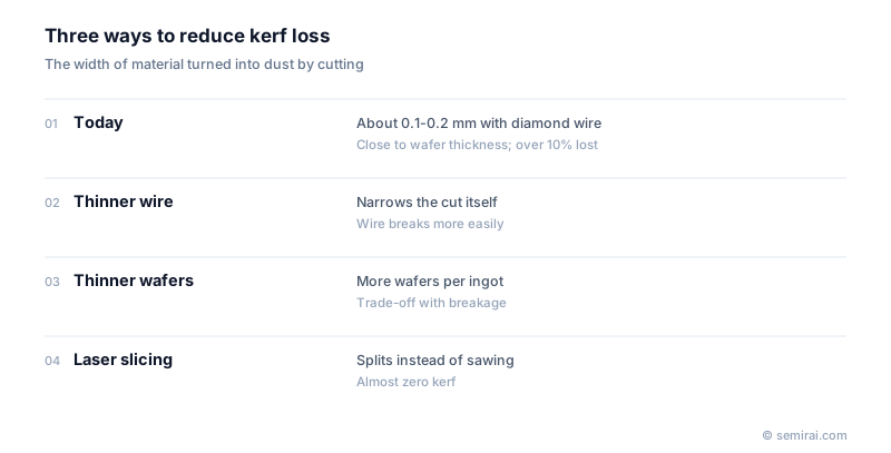
Kerf loss is the width of material removed and lost as dust when a cut is made. When an ingot is sliced with a diamond wire saw, the kerf is typically about 0.1-0.2 mm, which is of the same order as the thickness of a finished 300 mm silicon wafer (775 µm). More than a tenth of the crystal can disappear in slicing alone.
Also called: kerf, cutting loss, saw kerf
Diagram
Why kerf matters
The number of wafers an ingot yields is roughly its usable length divided by the sum of wafer thickness, kerf and polishing allowance. If a 775 µm wafer costs 150 µm of kerf, about 16% of the crystal is lost in cutting. Reducing kerf therefore increases output without buying or growing more crystal.
The silicon dust (kerf sludge) is mixed with abrasive and cutting fluid, so it cannot simply be reused as high-purity feedstock. Recovery methods have been studied, but they rarely pay off, so most of it is discarded. Cutting less is usually the better approach.
Three ways to reduce it
Thinner wire: a thinner diamond wire core narrows the cut, but the wire breaks more easily and tension becomes harder to control. Thinner wafers: more wafers fit in the same length, but warp and breakage during handling set a limit. A different cutting method: laser slicing separates the wafer along a modified layer inside the crystal and creates almost no kerf.
Kerf is most serious for SiC. The material is expensive, the ingots are only a few tens of millimetres long, and the hardness makes sawing slow. This is why laser slicing has been developed most actively for SiC, where it directly affects device cost.
Japanese companies involved
- DISCO developed KABRA, a laser process for slicing SiC ingots that aims to cut kerf loss and increase the number of wafers per ingot.
- Tokyo Seimitsu (ACCRETECH) makes wafer grinding machines used after slicing, where the removal allowance adds to the material lost in cutting.
- DISCO · Dicing, grinding and polishing equipment
- Tokyo Seimitsu (ACCRETECH) · Wafer probers, dicing and grinding machines, metrology
FAQ
Is kerf the only material lost between ingot and wafer?
No. Grinding, lapping, etching and polishing also remove material from both faces to clear saw damage and reach the final flatness. The total loss from ingot to finished wafer is therefore larger than the kerf alone.
Does kerf matter in dicing too?
Yes. When a processed wafer is cut into chips, the blade width sets how wide the streets between chips must be. Narrower kerf or kerf-free methods such as stealth dicing allow more chips per wafer, especially for small dies.
Related pages
- Wire Saw
- Laser Slicing / Laser Lift-off
- Silicon Ingot
- Wafer Thinning
- SiC Wafer (Silicon Carbide Substrate)
- Silicon Wafer Manufacturing
- Scribe Line
- Wire saws and wafer slicing equipment
- Tokyo Seimitsu (ACCRETECH) C-RW Series
- Asahi Diamond Industrial ECOMEP diamond wire
- Komatsu NTC MWM3050nQ
- Komatsu NTC MWM442DM
Sources
Last updated: November 13, 2026