Self-Alignment
Self-alignment is a manufacturing technique that uses a structure already on the wafer as a mask or guide, so the next feature is positioned automatically rather than by aligning a new lithography exposure. Every exposure carries some overlay error, but a self-aligned feature is fixed relative to the existing structure, so no margin for that error is needed.
Also called: self-aligned process, self-aligned gate
Diagram
The self-aligned gate
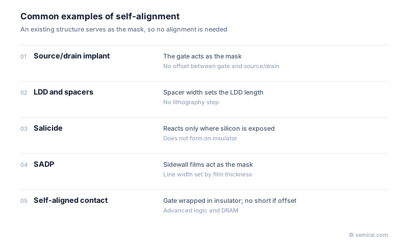
The best-known example is the self-aligned gate of the MOS transistor. The gate electrode is made first and then used as the mask for ion implantation, so the source and drain form right at its edges. When gates and source/drain regions were defined by separate exposures, they had to overlap to allow for misalignment, which added parasitic capacitance. Self-alignment removed that overlap and made transistors faster and smaller.
The same idea appears in sidewall spacers on the gate, which set the offset between lightly doped drain (LDD) regions and the main source/drain implant without an extra mask. It also appears in salicide (self-aligned silicide), where metal reacts with silicon only where silicon is exposed, so silicide forms on the gate and source/drain but not on the insulator.
Self-alignment at advanced nodes
Self-aligned contacts (SAC) wrap the gate in insulator so that a contact that lands slightly off target does not short to it. Self-aligned double and quadruple patterning (SADP, SAQP) use films grown on the sidewalls of lithographically printed lines to halve or quarter the pitch. Self-aligned vias are positioned by the metal lines above and below them.
In each case, deposition and etch make up for the limits of lithographic resolution and alignment, which is why self-alignment is used at so many steps in current logic and memory processes.
Japanese companies involved
- Tokyo Electron supplies deposition and etch systems used in self-aligned patterning steps such as spacer formation for SADP.
- Tokyo Electron (TEL) · Coat/develop, etch and deposition equipment
FAQ
What is the main benefit of self-alignment?
It removes the dependence on overlay accuracy for the self-aligned feature. Designers no longer need a safety margin for misalignment, so cells can be smaller, and device characteristics vary less because the feature position does not shift from wafer to wafer.
Does self-alignment eliminate lithography?
No. At least one patterning step is still needed to define the first structure, and some layers still require separate exposures. Self-alignment reduces the number of critical alignments and lets deposition thickness, rather than exposure, set some dimensions.
Related pages
Sources
Last updated: November 2, 2026