Shallow Trench Isolation (STI)
Shallow trench isolation (STI) is the technique of electrically isolating neighbouring transistors by etching shallow trenches into the silicon substrate and filling them with an insulator, usually silicon oxide. It replaced LOCOS isolation from around the 0.25 µm generation because it allows tighter packing and a flatter surface, and it is one of the first major modules in a CMOS process.
Also called: STI, trench isolation
Diagram
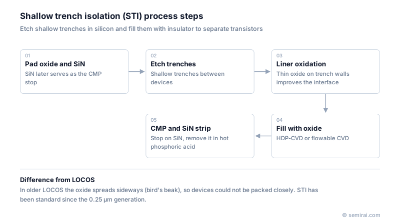
Process flow
A thin pad oxide and a silicon nitride layer are deposited, patterned and etched to open the isolation areas, and trenches are dry-etched into the silicon, typically a few hundred nanometres deep in planar CMOS. A thin liner oxide is grown on the trench walls to repair etch damage and round the top corners. The trench is then filled with oxide, first by high-density plasma CVD and, as trenches became narrower and deeper, by sub-atmospheric or flowable CVD, followed by an anneal to densify it.
Chemical mechanical polishing (CMP) removes the excess oxide and stops on the nitride, which acts as a polish stop. Finally the nitride is stripped in hot phosphoric acid and the pad oxide is removed, leaving active silicon areas separated by oxide-filled trenches.
Why STI replaced LOCOS
LOCOS grows thick oxide wherever nitride does not mask the wafer, but the oxide also grows sideways under the nitride edge in a tapering 'bird's beak'. This wastes area and limits how closely transistors can be placed, and the raised oxide makes the surface uneven. STI defines the isolation width by lithography and etching instead, and CMP leaves a nearly flat surface for gate patterning.
Problems and the role in FinFETs
The trench corner is sensitive. If wet cleans etch the fill oxide back below the silicon surface, a divot forms, the gate wraps around the corner and a parasitic corner transistor turns on early. Voids in the fill and dishing during CMP are other failure modes. The oxide also stresses the nearby silicon, changing carrier mobility depending on layout, an effect designers must account for.
In FinFETs, the oxide between fins is recessed after filling, and the recess depth sets how much of each fin sticks out above the isolation. Because exposed fin height determines drive current, this recess must be controlled to within a few nanometres.
Japanese companies involved
- Tokyo Electron supplies etch, deposition and cleaning equipment used in trench formation and fill.
- Ebara makes CMP systems used to planarise the oxide fill, and Resonac makes CMP slurries, including ceria-based slurries used for STI polishing.
- Ebara · CMP systems, dry vacuum pumps and exhaust treatment
- Resonac · CMP slurries, packaging materials and SiC epitaxial wafers
- Tokyo Electron (TEL) · Coat/develop, etch and deposition equipment
FAQ
Why is ceria slurry used for STI CMP?
STI polishing must remove oxide quickly but stop sharply on the nitride, and it must not dish wide oxide areas. Ceria-based slurries polish oxide much faster than nitride and can be formulated to slow down once the surface is flat, giving better selectivity and planarity than conventional silica slurries.
What is dummy fill in STI?
CMP removes material faster in regions with little active area, so large isolation areas dish while dense areas stay high. Layout tools add non-functional active squares, called dummy fill, to even out pattern density and keep the polished surface uniform across the chip.
Related pages
Sources
Last updated: November 2, 2026