Semiconductor
A semiconductor is a material whose electrical conductivity lies between that of metals and insulators and, more importantly, can be controlled. Adding tiny amounts of impurities (doping), or applying a voltage, light or heat, changes its conductivity by many orders of magnitude, which is what makes transistors, memory, sensors and solar cells possible.
Also called: semiconductor material, chip
Diagram
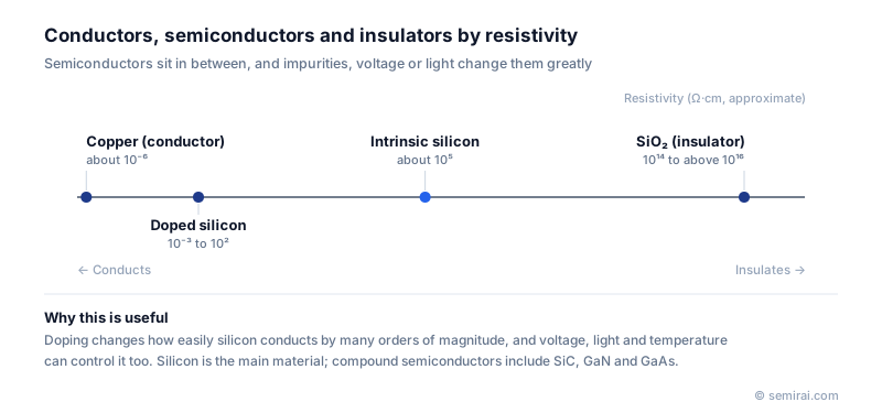
Why a semiconductor conducts only sometimes
In a solid, electrons occupy energy bands. In a semiconductor the valence band is full and the conduction band is almost empty, separated by a band gap of about 1.1 eV in silicon. At room temperature only a few electrons gain enough thermal energy to cross the gap, so pure silicon has a resistivity of roughly 10⁵ Ω·cm, around a hundred billion times that of copper. Unlike a metal, a semiconductor conducts better as it gets hotter, because more electrons are excited across the gap.
Doping changes this picture. Phosphorus or arsenic, often at well under one atom per million, adds free electrons and make n-type material; boron removes electrons from bonds, creating mobile holes and p-type material. The resistivity of silicon can be set anywhere from about 10⁻³ to 10² Ω·cm this way, precisely and region by region.
Main semiconductor materials
Silicon dominates because it is abundant, can be grown as large, nearly perfect single crystals (today 300 mm wafers), and forms a stable insulating oxide, SiO₂, by simple heating. Germanium was used for the first transistors and now appears mainly as SiGe alloys. Compound semiconductors fill roles silicon cannot: GaAs and InP for radio-frequency and optical devices, and the wide-bandgap materials SiC and GaN for power switching and, in GaN's case, blue and white LEDs. Materials with a direct band gap, such as GaAs and GaN, emit light efficiently; silicon does not.
From material to chip
Joining p-type and n-type regions forms a pn junction, the basis of diodes, bipolar transistors, LEDs and solar cells. In CMOS (complementary metal-oxide-semiconductor) technology, n-channel and p-channel MOSFETs are paired so that almost no current flows except while switching, which is why billions of transistors can share one chip. The resulting products include logic (CPUs, GPUs, FPGAs), memory (DRAM, NAND flash), analog and mixed-signal ICs, power devices, optoelectronics and sensors.
A chip is built on a wafer through hundreds of steps: lithography, etching, deposition, ion implantation, cleaning and planarisation are repeated layer by layer before the wafer is tested, diced and packaged.
Japanese companies involved
- Shin-Etsu Chemical and SUMCO grow single-crystal silicon and make the polished and epitaxial wafers on which chips are built.
- Tokyo Electron makes coater/developers, etch and deposition equipment used throughout front-end wafer processing.
- Kioxia makes NAND flash memory and Sony Semiconductor Solutions makes CMOS image sensors at fabs in Japan.
- Shin-Etsu Chemical · Silicon wafers, photoresists and photomask blanks
- SUMCO · Silicon wafers
- Tokyo Electron (TEL) · Coat/develop, etch and deposition equipment
- Kioxia · NAND flash memory and SSDs
- Sony Semiconductor Solutions · CMOS image sensors
FAQ
Why is silicon the most widely used semiconductor?
Silicon is the second most abundant element in the Earth's crust, its band gap suits room-temperature electronics, and it grows into large dislocation-free crystals. Its thermal oxide is an excellent insulator with a clean interface, which made the MOS transistor practical. Decades of process development have added to that lead.
Does 'semiconductor' mean the material or the chip?
Strictly it names the material class. In industry and news, 'semiconductors' usually means the devices made from those materials, from discrete transistors to processors, and by extension the industry that makes them.
Where is the line between a semiconductor and an insulator?
There is no sharp boundary. Materials with gaps up to a few electron volts that can be doped to control their conductivity are treated as semiconductors; SiC and GaN qualify even with gaps above 3 eV. SiO₂, with a gap of about 9 eV, cannot usefully be doped and is an insulator.
Related pages
Sources
Last updated: November 2, 2026