Sidewall Spacer
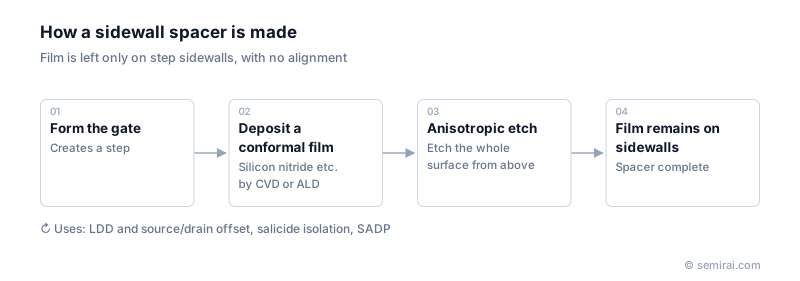
A sidewall spacer is a thin wall of insulating film, usually silicon nitride or silicon oxide, left on the sides of a step such as a transistor gate. A film is deposited evenly over the step and then etched straight down by anisotropic dry etching. The film on flat areas is removed, but the film on the sidewalls remains, with no lithographic alignment needed.
Also called: gate spacer, spacer
Diagram
Roles in the transistor
The main role is to set the position of the source and drain implants. Before the spacer is formed, a shallow, lightly doped region called the lightly doped drain (LDD) is implanted next to the gate. After the spacer is formed, the heavy source/drain implant is done, and the spacer keeps it a fixed distance from the gate edge. This softens the electric field at the drain end of the channel and reduces hot-carrier degradation.
In the salicide step, metal silicide forms only on exposed silicon. The spacer covers the gate sides, so silicide on the gate and on the source/drain does not join and short the transistor.
Spacers for pitch splitting
Self-aligned double patterning (SADP) uses the same technique to make features smaller than lithography can print. Spacers are formed on both sides of a printed line, called the mandrel or core, and the mandrel is then removed. Two spacer lines remain for each original line, doubling line density. The pattern is transferred to the layer below.
SADP and its extension, self-aligned quadruple patterning (SAQP), are used to form FinFET fins and dense memory and logic wiring. Because spacer width is set by film thickness, atomic layer deposition (ALD) is often used to control it precisely.
Japanese companies involved
- Tokyo Electron and Kokusai Electric supply deposition equipment, including ALD systems, used to form spacer films.
- Tokyo Electron (TEL) · Coat/develop, etch and deposition equipment
- Kokusai Electric · Batch deposition, diffusion and ALD equipment
FAQ
Why does the film remain only on the sidewalls?
A conformal film is much thicker in the vertical direction along a sidewall than on flat surfaces. Anisotropic etching removes the same vertical thickness everywhere, so it clears the flat areas while the sidewall film, being taller, is only partly consumed and remains as a spacer.
What limits the precision of SADP?
Line width depends on spacer thickness, which deposition can control well, but the spacing between lines also depends on the mandrel width and etch profile. Variation in the mandrel splits lines into two slightly different groups, an effect called pitch walking, which process control has to minimise.
Related pages
Sources
Last updated: November 13, 2026