Area-Selective Deposition (ASD)
Area-selective deposition (ASD) is a technique that deposits a film only on chosen materials on the wafer surface and not on others, for example a cap only on metal lines and not on the surrounding dielectric. Because the film's position is set by the existing surface rather than by lithography and etch, it is also called bottom-up patterning.
Also called: ASD, selective deposition, bottom-up patterning
Diagram
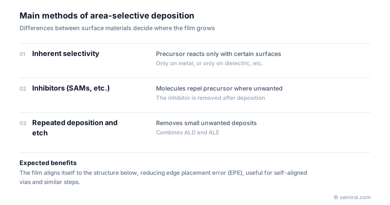
How selectivity is achieved
There are three main approaches. The first uses inherent selectivity: some precursors react readily with one surface, such as a metal, but hardly with another. The second uses inhibitors: molecules that block the precursor, such as self-assembled monolayers (SAMs) or small-molecule inhibitors, are first adsorbed where no film is wanted, then removed after deposition.
The third corrects imperfect selectivity. Over many cycles a little film nucleates where it should not, so deposition is alternated with short etch steps, for example atomic layer deposition (ALD) with atomic layer etching (ALE), to clear the unwanted nuclei while the intended film keeps growing. In practice, several methods are often combined.
Why chipmakers are interested
At advanced nodes, overlay errors between lithography layers and variations in feature size move pattern edges away from their intended positions. This edge placement error (EPE) limits yield and design rules. ASD aligns new material automatically to the structure below, so it can widen the margin for steps such as fully self-aligned vias, where a via must land exactly on the line beneath.
ASD might also remove some lithography and etch steps and lower cost. The barriers to volume production are keeping selectivity over a useful film thickness and achieving very low defect levels across a full wafer.
Japanese companies involved
- Tokyo Electron (TEL) · Coat/develop, etch and deposition equipment
FAQ
How does the inhibitor method work?
A molecule that does not react with the deposition precursor is adsorbed on the surface where no film is wanted. During the following ALD or CVD step the precursor cannot attach there, so the film forms only on the uncovered surface. The inhibitor is then removed, often by a plasma or thermal step.
How is selectivity measured?
Selectivity is usually given as the amount deposited on the growth surface compared with the non-growth surface after a given number of cycles. Surface analysis such as XPS and defect inspection on patterned wafers show how many unwanted nuclei have formed and how thick the film can grow before selectivity is lost.
Related pages
Sources
Last updated: November 1, 2026