Multi-Patterning
Multi-patterning is a set of techniques that form features finer than a single lithography exposure can resolve by splitting the pattern across several exposures or by using deposited spacers to multiply line density. It let 193 nm ArF immersion lithography produce the 10 nm and 7 nm logic nodes before EUV entered volume production.
Also called: multiple patterning, double patterning, LELE, SADP, SAQP
Diagram
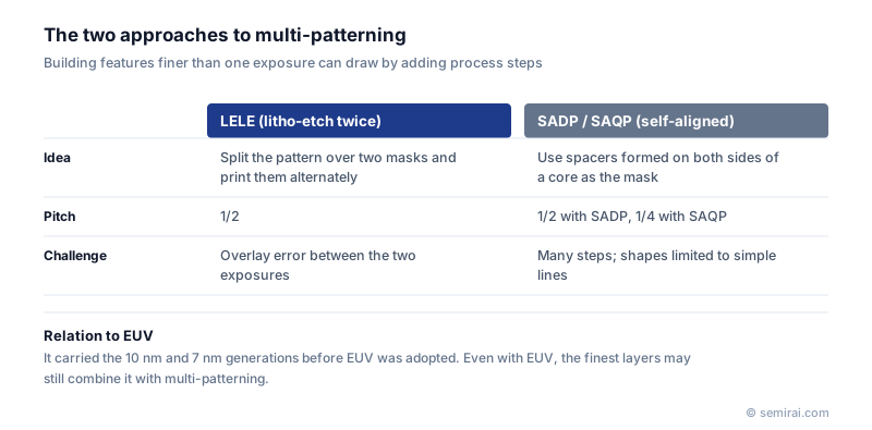
Why one exposure is not enough
The smallest pitch a scanner can print in one exposure is set by the wavelength and numerical aperture (NA). For ArF immersion, with a 193 nm wavelength and an NA of 1.35, the practical limit is a pitch of roughly 80 nm. Advanced logic and memory needed much tighter metal and fin pitches, and EUV was not yet ready, so the industry learned to build those pitches from several coarser steps.
The main methods
LELE (litho-etch-litho-etch) splits a layout into two masks whose features interleave. The first pattern is exposed and etched into a hard mask, then the second is exposed and etched between the first, halving the pitch. Any placement error between the two exposures directly shifts one set of lines against the other, so LELE demands very tight overlay control. Triple and quadruple variants (LE3, LE4) extend the idea with more masks. The layout must also be split, or coloured, so that neighbouring features land on different masks.
Self-aligned double patterning (SADP) prints a core pattern, called a mandrel, then deposits a thin conformal spacer film over it, usually by atomic layer deposition. An anisotropic etch leaves the film only on the mandrel sidewalls, and the mandrel is removed. Each mandrel line has produced two spacer lines, so the pitch is halved, and the spacing is set by film thickness rather than by the scanner. Repeating the sequence on the first spacers gives self-aligned quadruple patterning (SAQP) at a quarter of the original pitch. Spacer methods suit regular line arrays such as fins and metal tracks; cuts and blocks with separate masks then define where lines end.
Costs and the role of EUV
Every extra exposure, deposition and etch adds cost, cycle time and sources of variation. With LELE, overlay errors accumulate; with spacer methods, spacer thickness uniformity and etch selectivity during mandrel removal decide line width. Design rules also become restrictive because only certain shapes can be split cleanly.
EUV, at 13.5 nm, replaced many ArF multi-patterning steps from the 7 nm generation onward with single exposures. Multi-patterning has not disappeared: ArF SAQP is still used for regular arrays, and the tightest layers of the most advanced logic combine EUV with double patterning.
Japanese companies involved
- Tokyo Electron supplies coater/developers, deposition and etch systems used in spacer-based multi-patterning sequences.
- Nikon makes ArF immersion scanners, the exposure tools on which ArF multi-patterning is built.
- Nikon · ArF, KrF and i-line lithography systems
- Tokyo Electron (TEL) · Coat/develop, etch and deposition equipment
FAQ
What is the difference between LELE and SADP?
LELE uses two separate exposures, so its accuracy depends on overlay between them and it can print fairly free shapes. SADP uses one exposure plus a deposited spacer, so line spacing is self-aligned and very uniform, but it naturally produces simple parallel lines that must be cut afterwards.
Is multi-patterning still needed with EUV?
For the finest pitches, yes. A single EUV exposure at today's NA cannot print every critical layer of the newest logic nodes, so some layers use EUV double patterning. High-NA EUV aims to bring those layers back to a single exposure.
Why does multi-patterning raise wafer cost so much?
Each patterning stage needs its own lithography pass, hard-mask deposition, etch, clean and metrology. A layer built with SAQP can take many more process steps than one exposed once, which also lengthens the time a wafer spends in the fab.
Comparisons
Related pages
Sources
Last updated: November 2, 2026