Smart Cut
Smart Cut is a technology that transfers a very thin single-crystal layer from one wafer to another by combining hydrogen ion implantation with wafer bonding. It was developed at the French research institute CEA-Leti in the 1990s and commercialised by Soitec as a production method for silicon-on-insulator (SOI) wafers. Most SOI wafers today are made this way.
Also called: Smart Cut process, ion-cut, layer transfer
Diagram
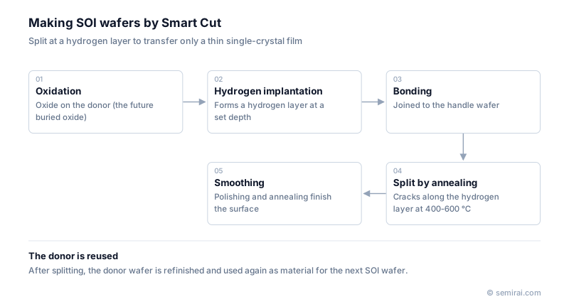
How the process works
First, the donor wafer is oxidised, and hydrogen ions are implanted to form a hydrogen-rich layer at a set depth below the surface. The donor is then bonded face down to a second wafer, the handle. When the bonded pair is heated to roughly 400-600 °C, the donor splits along the hydrogen layer, leaving a thin silicon layer and the oxide on the handle wafer. Finally, the split surface is smoothed by polishing and annealing.
The oxide grown on the donor becomes the buried oxide (BOX) of the SOI wafer.
Advantages and wider uses
The implant depth precisely sets the thickness of the transferred layer, so Smart Cut suits wafers that need a very thin, uniform silicon layer, such as fully depleted SOI (FD-SOI), where the layer is around 10 nm thick. After the split, the donor wafer can be refinished and used again, so little material is wasted.
The method has spread beyond silicon. It is used to transfer thin layers of costly SiC onto cheaper supporting substrates, and to make bonded substrates with piezoelectric materials such as lithium tantalate for RF filters.
Japanese companies involved
- Shin-Etsu Chemical's group produces SOI wafers, including by the Smart Cut process under licence from Soitec.
- Shin-Etsu Chemical · Silicon wafers, photoresists and photomask blanks
FAQ
Why does the wafer split at the hydrogen layer?
Implanted hydrogen forms tiny cavities in the crystal. On heating, the hydrogen becomes gas, pressure in the cavities rises and they link up into a crack that runs through the whole layer. The bonded handle wafer supports the thin layer so it transfers without breaking.
What other ways are there to make SOI wafers?
SIMOX implants a large dose of oxygen ions and anneals at high temperature to form the buried oxide. Bond-and-etch-back SOI (BESOI) bonds two wafers and thins one by grinding and polishing. Smart Cut stands out for thin-layer uniformity and donor wafer reuse.
Comparisons
Related pages
Sources
Last updated: November 2, 2026