SOI (Silicon on Insulator)
SOI (silicon on insulator) is a substrate technology in which a buried oxide layer (BOX) separates a thin top layer of silicon from the silicon substrate below, and transistors are built in the top layer. Because each device is electrically isolated from the substrate, SOI reduces junction capacitance and leakage, prevents latch-up and improves radiation tolerance.
Also called: SOI wafer, FD-SOI, RF-SOI
Diagram
Partially and fully depleted SOI
In partially depleted SOI (PD-SOI), the top silicon is thick enough that only part of it is depleted under the gate. The undepleted body floats electrically, which causes history effects: the transistor's behaviour depends on how it was switched before.
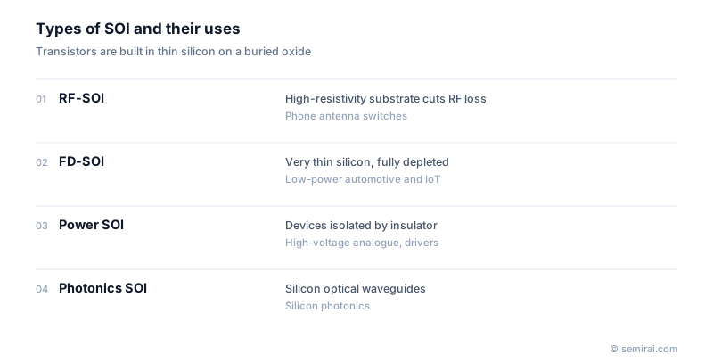
In fully depleted SOI (FD-SOI), the top silicon is so thin, typically under about 10 nm, that the whole channel is depleted. The channel needs little or no doping, short-channel effects are suppressed, and a voltage applied to the substrate below the BOX (body bias) can shift the threshold voltage while the chip is running. This makes FD-SOI attractive for low-power microcontrollers, IoT chips and RF circuits. STMicroelectronics and GlobalFoundries (22FDX) manufacture FD-SOI processes.
Other types and how SOI wafers are made
RF-SOI uses a high-resistivity substrate to reduce signal loss and is widely used for antenna switches and tuners in smartphones. Thicker SOI is used to isolate high-voltage drivers and analogue circuits, and photonics SOI provides the silicon waveguide layer for silicon photonics.
Most SOI wafers are made by layer transfer. In Soitec's Smart Cut process, hydrogen ions are implanted into an oxidised wafer, the wafer is bonded to a second wafer, and it is split along the implanted layer, leaving a thin silicon film on the oxide. The donor wafer can be reused. Bonding followed by grinding and polishing (BESOI) is used for thicker layers.
Japanese companies involved
- Shin-Etsu Chemical's wafer business and SUMCO, both major silicon wafer makers, also produce SOI wafers.
- Shin-Etsu Chemical · Silicon wafers, photoresists and photomask blanks
- SUMCO · Silicon wafers
FAQ
Why is SOI resistant to radiation and latch-up?
In bulk silicon, a particle strike generates charge deep in the substrate that can be collected by a transistor, and parasitic paths through the substrate can trigger latch-up. With a buried oxide, the active volume is tiny and isolated, so less charge is collected and the parasitic thyristor path does not exist. This is why SOI is used in space and other harsh environments.
Does FD-SOI compete with FinFET?
They are two different answers to short-channel effects. FinFET wraps the gate around a fin and scales to the most advanced nodes. FD-SOI keeps a planar transistor on a thin film, which is simpler to design and offers body bias, so it is chosen for low-power and RF chips at nodes such as 28 nm and 22 nm.
Comparisons
Related pages
Sources
Last updated: November 2, 2026