SiC Wafer (Silicon Carbide Substrate)
A SiC wafer is a single-crystal silicon carbide substrate on which SiC power devices are built. Unlike silicon, SiC cannot be pulled from a melt, so the crystal is grown by sublimation above 2,000 °C and recrystallisation on a seed. Slow growth, crystal defects and very hard material make the wafers expensive.
Also called: silicon carbide wafer, SiC substrate, 4H-SiC wafer
Diagram
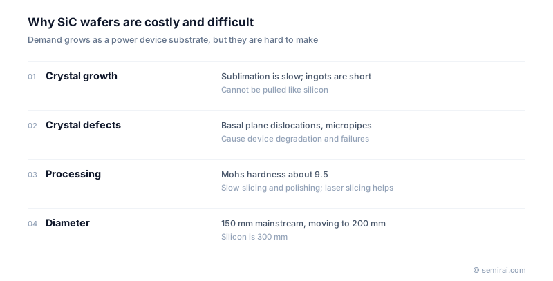
Why SiC substrates are difficult
SiC does not melt at normal pressure, so the Czochralski method used for silicon is not possible. The crystal is grown by physical vapour transport (PVT): SiC powder is sublimated and the vapour crystallises on a slightly cooler seed. Growth is slow and the ingots are short, so each furnace run yields far fewer wafers than a silicon ingot.
Diameter has also grown slowly. 150 mm wafers were the mainstream for a long time, and the industry is now moving to 200 mm, while silicon has been made at 300 mm for many years. Fewer chips per wafer and fewer wafers per ingot both raise cost.
Defects and processing
SiC has its own crystal defects. Micropipes, hollow cores running through the crystal, were once a major problem and have been greatly reduced. Basal plane dislocations (BPDs) remain important: under forward current they can expand into stacking faults and raise on-resistance over time. During epitaxial growth, most BPDs are converted into less harmful threading edge dislocations.
SiC is one of the hardest materials in use, behind diamond, so slicing, grinding and polishing take long and lose a lot of material. Laser slicing, which separates a wafer along a modified layer inside the ingot instead of sawing, is being introduced to cut this loss.
Japanese companies involved
- Resonac and Sumitomo Electric Industries produce SiC epitaxial wafers for power devices, and ROHM makes SiC substrates through its group company SiCrystal and uses them for its own SiC MOSFETs and diodes.
- DISCO developed KABRA, a laser slicing process for SiC ingots, and Komatsu NTC and Takatori make wire saws used to slice SiC.
- DISCO · Dicing, grinding and polishing equipment
- Komatsu NTC · Wire saws for slicing silicon and SiC ingots
- Takatori · Wire saws, dicing-related equipment and bonding/debonding systems
- Resonac · CMP slurries, packaging materials and SiC epitaxial wafers
- Sumitomo Electric Industries (compound semiconductors) · SiC epitaxial wafers and GaAs and InP substrates
- ROHM · SiC and silicon power devices, analog ICs
- Mitsuboshi Diamond Industrial · Scribe-and-break cutting systems and scribing wheels
FAQ
Why are SiC wafers so much more expensive than silicon wafers?
Crystal growth by sublimation is slow and gives short ingots, the defects specific to SiC limit usable yield, and the extreme hardness makes slicing and polishing slow. Smaller diameters then mean fewer chips per wafer.
What polytype is used for power devices?
Almost all SiC power devices use the 4H polytype, which has a wide band gap and high electron mobility along the c-axis. Growth conditions must be controlled to avoid other polytypes such as 6H forming inside the crystal.
Are devices built directly on the substrate?
No. A thin epitaxial SiC layer with precisely controlled doping is grown on the substrate first, and the devices are formed in that layer. The substrate mainly provides mechanical support and a conducting back contact.
Comparisons
Related pages
- Silicon Carbide (SiC)
- Silicon Wafer
- SiC MOSFET (Silicon Carbide MOSFET)
- Power Semiconductor
- Epitaxy (Epitaxial Growth)
- Wide Bandgap Semiconductor (WBG)
- Gallium Nitride (GaN)
- Breakdown Voltage
- Power semiconductor manufacturing equipment
- Advantest EXAVIS
- Advantest MT100 / MT200
- Hitachi High-Tech M-600 / 6000 series
Sources
Last updated: November 2, 2026