Substrate
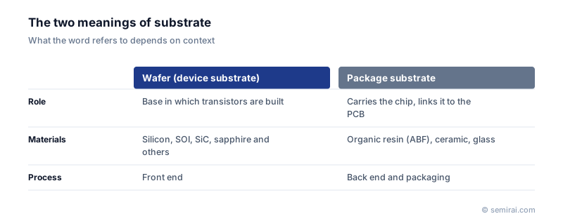
A substrate is the base on which films are formed, devices are built or components are mounted. In semiconductors the word has two main meanings: the wafer in which transistors are made, and the package substrate that carries the chip and connects it to the printed circuit board. Which one is meant depends on context.
Also called: base material, wafer, package substrate
Diagram
The substrate in front-end processing
In wafer fabrication, the substrate is the wafer itself. Most chips are built on single-crystal silicon. Depending on the application, other substrates are used: silicon-on-insulator (SOI), with a thin silicon layer on an insulating film; silicon carbide (SiC) for power devices; and sapphire, gallium arsenide (GaAs) or indium phosphide (InP) for LEDs, lasers and RF devices.
The substrate is more than a mechanical support. It is the template for any crystal grown on it. If the lattice constant or thermal expansion of the substrate and the film do not match, the epitaxial film develops dislocations and the wafer warps. In transistor physics, 'substrate' also refers to the body terminal, as in substrate bias or back-gate bias.
The substrate in packaging
In back-end processing, the substrate is the package substrate: the interposing board that holds the chip and routes its connections to the printed circuit board. In ball grid array (BGA) packages, organic substrates built from stacked resin insulating layers, such as ABF film, and copper wiring are the mainstream. For large AI processors, the fineness of the wiring and the size of the substrate have become limits on both performance and supply.
Glass-core substrates, which warp less and suit finer wiring, are being developed as a next-generation option. Power modules use insulating ceramic substrates, such as direct bonded copper (DBC) substrates with copper bonded to ceramic.
Japanese companies involved
- Shin-Etsu Chemical and SUMCO make silicon wafers, the most common device substrate.
- IBIDEN makes FC-BGA package substrates for high-performance processors, and Kyocera makes organic and ceramic package substrates.
- Shin-Etsu Chemical · Silicon wafers, photoresists and photomask blanks
- SUMCO · Silicon wafers
- IBIDEN · IC package substrates (FC-BGA)
- Kyocera · Package substrates and ceramic components
FAQ
How can I tell which kind of substrate is meant?
Look at the process step. Discussions of crystal growth, doping, film deposition or transistor physics refer to the wafer. Discussions of packaging, bumps, build-up layers or board assembly refer to the package substrate. In deposition, 'substrate' can also simply mean whatever surface the film is deposited on.
What is substrate bias?
It is a voltage applied to the body of the wafer under a transistor. Changing it shifts the transistor's threshold voltage, an effect used deliberately in some designs, especially on thin SOI wafers, to trade speed against leakage.
Related pages
- Silicon Wafer
- SOI (Silicon on Insulator)
- Sapphire Substrate
- SiC Wafer (Silicon Carbide Substrate)
- Epitaxial Wafer (Epi Wafer)
- Package Substrate
- Compound Semiconductor
- GaN-on-Silicon (GaN-on-Si)
- Compound semiconductor substrate equipment (SiC/GaN)
- Daiichi Kiden Solution Growth System
- Fujikoshi Machinery LSL-19A
- Hamai Industries HS1200
- Okamoto Machine Tool Works OGM390NC2HX
Sources
Last updated: November 13, 2026