Wafer-Level Burn-In (WLBI)
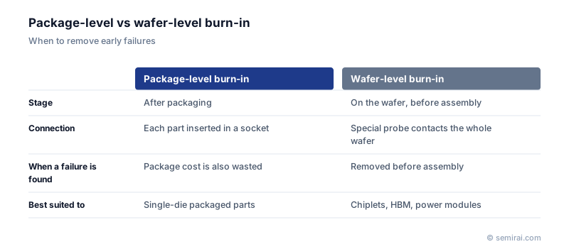
Wafer-level burn-in (WLBI) applies high temperature and high voltage to chips while they are still on the wafer, before packaging, to remove those likely to fail early. Burn-in screens out infant-mortality failures before shipment; it was traditionally done on packaged chips placed one by one in sockets.
Also called: WLBI, wafer burn-in
Diagram
Why burn in at wafer level
Finding weak chips earlier saves money. If a chip fails burn-in after packaging, the package materials and assembly work are wasted as well.
The benefit is largest for products that combine many dies in one package, such as chiplet designs, HBM stacks and power modules. A single bad die can scrap the whole assembly, so it is important to start with known good dies (KGD) that have already been stressed and tested.
Technical challenges
WLBI needs a special contactor that connects to all the chips across the wafer at once, and a way to heat the wafer evenly. Because hundreds to thousands of chips are powered at the same time, current delivery and heat management are difficult, and a shorted die must not disturb its neighbours.
SiC MOSFETs for electric vehicles are a growing use. Their gate oxide on silicon carbide is prone to early defects, and an inverter module uses many dies, so stressing the gate at wafer level before assembly improves module yield and reliability.
Japanese companies involved
- H.I. Systec and Shikino High-Tech make burn-in boards and related equipment for conventional package-level burn-in, the step that wafer-level burn-in partly replaces.
- H.I. Systec · Burn-in boards, racks and test fixtures
- Shikino High-Tech · Burn-in boards, semiconductor test equipment and LSI design
- Advantest · Automated test equipment (ATE) for SoC and memory
FAQ
How does wafer-level burn-in differ from conventional burn-in?
Conventional burn-in loads packaged parts into sockets on burn-in boards and stresses them in an oven. Wafer-level burn-in contacts every die on an unpackaged wafer at once. It moves the screen earlier in the flow, so failing dies are discarded before any assembly cost is spent on them.
Why is WLBI used for SiC MOSFETs?
The interface between silicon carbide and its gate oxide contains more defects than in silicon, which leads to early gate failures. EV inverters use many SiC dies per module, so one early failure is costly. Stressing the gate on the wafer removes weak dies before they are mounted.
Related pages
Sources
Last updated: November 2, 2026