Burn-In Test
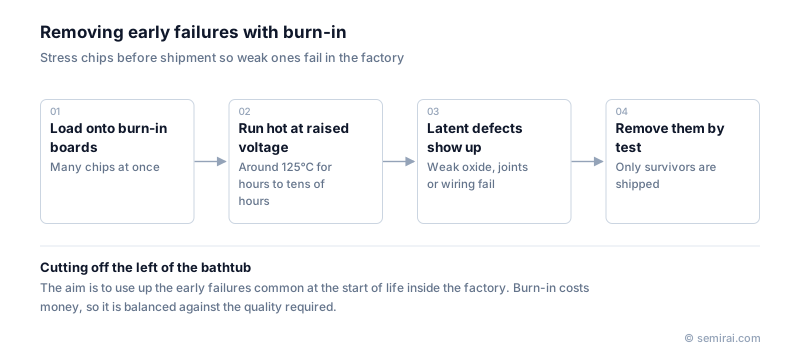
Burn-in is a screening step in which semiconductor devices are operated at high temperature and raised voltage before shipment, so that units with latent manufacturing defects fail early and are removed. A typical burn-in keeps devices powered at around 125°C for a few hours to a few tens of hours, then retests them and ships only the survivors.
Also called: burn-in, burn-in screening, dynamic burn-in
Diagram
Why burn-in works
The idea comes from the bathtub curve. The failure rate of a population of chips is high at the very start of use, falls to a low and roughly constant level, and rises again at the end of life as wear-out sets in. The early failures come from defects such as weak oxide, marginal contacts or thin interconnect spots that pass the normal electrical test but give way under stress.
Heat and voltage speed up the mechanisms that make these weak devices fail. A few hours of stress in the factory therefore consumes the early-failure part of the curve, and the parts that reach customers start their life in the flat, low-failure region. Automotive, aerospace and defence customers usually demand stricter burn-in conditions than consumer markets.
How burn-in is done
Many packaged devices are loaded onto burn-in boards (BIBs), which are placed in temperature-controlled ovens and powered in parallel. In static burn-in the devices are simply biased; in dynamic burn-in they are clocked and exercised, for example by repeatedly writing and reading memory arrays, so that more of the circuit is stressed.
Burn-in costs oven time, boards and floor space, so manufacturers try to shorten it. Reliability data from tests such as HTOL and statistical analysis are used to choose the shortest conditions that still give the required field quality. For stacked products such as HBM and multi-die packages, screening individual dies before assembly (known good die) has become more important, because one weak die can scrap a whole stack.
Japanese companies involved
- ESPEC, a Japanese maker of environmental test equipment, supplies temperature chambers and burn-in systems used for screening and reliability testing of semiconductor devices.
FAQ
Is burn-in the same as aging?
No. Aging usually means long operation at room temperature and rated voltage. Burn-in is an accelerated stress: temperature and voltage are raised so that weak devices fail within hours, and the equivalent field time is estimated with acceleration models such as the Arrhenius equation.
How is burn-in different from HTOL?
Both apply heat and voltage, but for different purposes. Burn-in is a screen applied to production parts to remove early failures. HTOL is a qualification test on a small sample, run for around 1,000 hours to estimate wear-out lifetime and failure rate.
Comparisons
Related pages
Sources
Last updated: November 2, 2026