Wafer Thinning
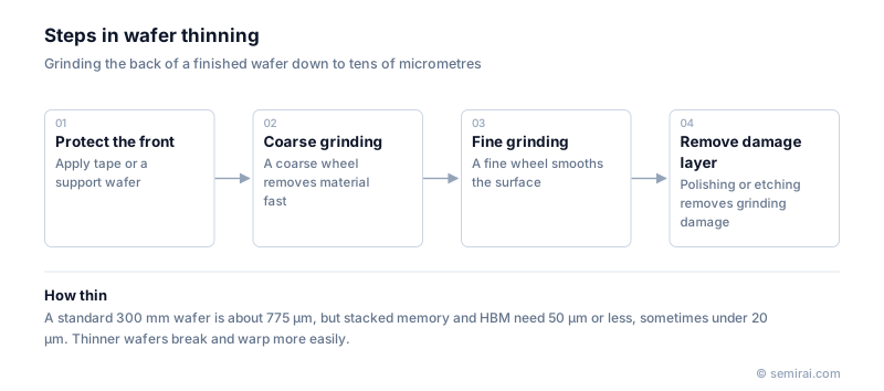
Wafer thinning is the removal of material from the back side of a finished wafer to reduce its thickness, mainly by grinding followed by polishing or etching. A standard 300 mm wafer is about 775 µm thick during front-end processing; packages commonly need dies of 100 to 200 µm, and stacked memory and 3D integration need 50 µm or less.
Also called: backside thinning, wafer back grinding
Diagram
Why wafers are thinned
Wafers are thick during processing so they stay flat and strong through hundreds of steps. Once the circuits are finished, most of that silicon is no longer needed. Thinner dies make thinner packages, conduct heat out more easily and, in power devices, lower the resistance of the substrate path. For stacking, thinning is essential: memory packages with many dies, HBM stacks and TSV wafers all require dies only a few tens of micrometres thick, and TSVs can only be exposed by thinning from the back.
The process steps
First, the circuit side is protected with a back-grinding tape or, for very thin targets and TSV wafers, by temporarily bonding the wafer to a rigid carrier. Coarse grinding with a diamond wheel then removes most of the material quickly, and fine grinding with a finer wheel reduces roughness and the depth of damage. Grinding leaves a thin layer of cracked and strained silicon that weakens the die, so a final stress-relief step removes it by CMP, dry polishing or wet or plasma etching.
After thinning, a TSV wafer goes on to backside via reveal, insulation, bumping and dicing while still on its carrier. Very thin wafers bow and break easily, so handling, transfer and chucking must be designed for them. In the TAIKO process developed by DISCO, only the inner area is ground and a thick ring is left at the edge to keep the wafer rigid; it is common for thin power-device wafers.
Thinning and dicing order
Thin wafers can chip and crack when diced. In dicing before grinding (DBG), grooves are cut part way into the front first, and grinding from the back separates the dies at the end, so a fragile thin wafer is never sawn. Stealth dicing, which forms a modified layer inside the silicon with a laser, can be combined with grinding in a similar way.
Japanese companies involved
- DISCO makes grinders, polishers and dicing saws used to thin and singulate wafers, and offers the DBG and TAIKO processes.
- Tokyo Seimitsu (ACCRETECH) makes grinding and polishing systems for wafer thinning.
- LINTEC and Nitto Denko supply back-grinding tapes that protect the circuit side during thinning.
- LINTEC · Dicing and backgrinding tapes, tape processing equipment
- Nitto Denko · Dicing tapes and functional films
- DISCO · Dicing, grinding and polishing equipment
- Tokyo Seimitsu (ACCRETECH) · Wafer probers, dicing and grinding machines, metrology
FAQ
How thin can a silicon wafer be ground?
Production processes thin wafers to around 20 to 50 µm for stacked memory and 3D integration, and research has gone thinner. At that thickness silicon becomes flexible, so the wafer must be supported by a carrier or tape throughout.
Does thinning weaken the die?
Grinding damage does. A die with its damage layer removed by polishing or etching can be strong even when thin, while an as-ground die cracks at much lower stress. That is why the stress-relief step matters as much as the grinding.
What is the difference between wafer thinning and a backgrinder?
Wafer thinning is the overall process, including protection, grinding, stress relief and handling. A backgrinder is the machine that performs the grinding, often combined with a polishing unit in one system.
Related pages
Sources
Last updated: November 2, 2026