Package Warpage
Package warpage is the bowing of a semiconductor package away from a flat shape, or the size of that deviation. A package bonds together silicon, mould compound, substrate and solder, which expand by different amounts, so a change in temperature makes the whole stack bend, in the same way as a bimetallic strip.
Also called: warpage, warping
Diagram
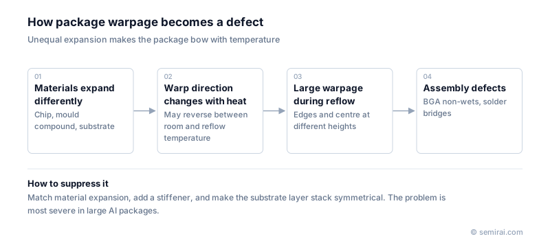
Why warpage changes with temperature
Warpage changes not only in size but often in direction as temperature changes. A package may be concave at room temperature and turn convex at the reflow peak of around 260°C, partly because the resins change behaviour at their glass transition temperature.
During reflow, large warpage causes typical BGA defects: some balls do not touch the solder paste and stay open (non-wet); neighbouring molten joints merge into bridges; or a ball rests on the paste without coalescing, which is called head-in-pillow. Warpage is therefore measured across the whole assembly temperature range, commonly with shadow moiré, which maps surface shape while the sample is heated and cooled.
Large AI packages and countermeasures
Warpage is a major issue for large AI packages. When a large die or interposer and several HBM stacks sit on one substrate, the footprint is big, so even a slight curvature produces a large displacement at the edges.
Engineers tune the CTE, modulus and Tg of mould compound and underfill, make the substrate layer build-up symmetrical, and attach a metal stiffener ring or lid to hold the package flat. Glass-core substrates, whose CTE can be brought close to silicon, are also being developed partly to control warpage.
Japanese companies involved
- Resonac and Sumitomo Bakelite develop mould compounds and underfills designed to reduce warpage.
- IBIDEN and Shinko Electric Industries manufacture large FC-BGA substrates, where layer design and core material are tuned to keep the package flat.
- Resonac · CMP slurries, packaging materials and SiC epitaxial wafers
- IBIDEN · IC package substrates (FC-BGA)
- Shinko Electric Industries · FC-BGA package substrates and lead frames
- Sumitomo Bakelite · Epoxy mold compounds and package materials
FAQ
How much warpage is acceptable?
Limits depend on package size, ball pitch and the agreement between supplier and assembler. Industry standards from JEDEC and JEITA describe how to measure warpage at temperature and give guidance values, and the allowed amount generally gets tighter as pitch gets finer.
Does the board also warp?
Yes. The printed circuit board deforms during reflow too, so what matters is the relative gap between package and board. Assemblers increasingly look at both shapes together when diagnosing open or bridged joints.
Related pages
Sources
Last updated: November 2, 2026