200mm Wafer (8-inch Wafer)
A 200mm wafer is a silicon wafer 200 mm (about 8 inches) in diameter. It became the main volume size in the 1990s, and even after leading-edge production moved to 300 mm in the 2000s, it remains widely used for power semiconductors, MEMS, sensors, analog ICs and display drivers.
Also called: 8-inch wafer, 200 mm wafer
Diagram
Specifications and handling
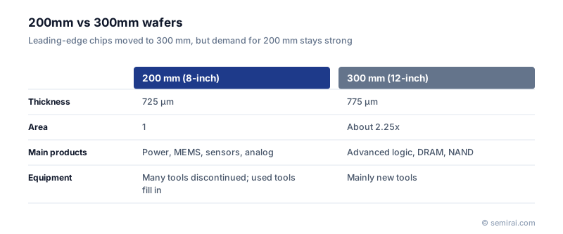
Under SEMI standards, a 200mm wafer is 725 µm thick. Crystal orientation is usually marked with a notch, a small V-shaped cut in the edge, whereas wafers of 150 mm and smaller mostly use a straight orientation flat.
Wafers are commonly handled in open cassettes combined with standard mechanical interface (SMIF) pods. Compared with 300 mm fabs, which assume fully automated transport with FOUPs and overhead hoists, 200 mm lines rely more on manual handling.
Equipment supply and demand
Many 200 mm tool models are out of production or available new only in limited numbers. Used equipment and tools refurbished by equipment makers therefore make up a large part of 200 mm equipment purchases.
Demand from vehicle electrification and industrial equipment has kept 200 mm capacity growing. Silicon carbide (SiC) power devices, which have long been made on 150 mm wafers, are also moving to 200 mm.
Japanese companies involved
- Shin-Etsu Chemical and SUMCO supply 200mm silicon wafers alongside 300mm wafers.
- Many Japanese power, sensor and analog device fabs run on 200 mm lines.
- Shin-Etsu Chemical · Silicon wafers, photoresists and photomask blanks
- SUMCO · Silicon wafers
FAQ
How many inches is a 200mm wafer?
About 8 inches (200 mm is 7.87 inches), so it is called an 8-inch wafer. In the same way, 300 mm wafers are called 12-inch and 150 mm wafers 6-inch.
Why not move everything to 300 mm?
Products such as power devices, sensors and analog ICs use mature processes and smaller volumes per design. Depreciated 200 mm fabs and used tools make them cheap to produce, and the gain from a larger wafer does not always justify building a new 300 mm line.
Is there a 200 mm SiC wafer?
Yes. SiC wafers have mainly been 150 mm, and the industry is moving to 200 mm to lower cost per chip, using 200 mm silicon-era equipment where possible.
Related pages
Sources
Last updated: November 2, 2026