300mm Wafer (12-inch Wafer)
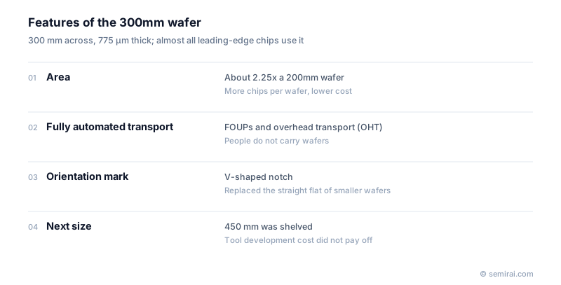
A 300mm wafer is a silicon wafer 300 mm (about 12 inches) in diameter. Volume production began in the early 2000s, and nearly all leading-edge logic, DRAM and NAND flash is now made on 300 mm wafers. Its area is about 2.25 times that of a 200mm wafer, so more chips come from each wafer and the cost per chip falls.
Also called: 12-inch wafer, 300 mm wafer
Diagram
Specifications and automation
Under SEMI standards, a 300mm wafer is 775 µm thick and its crystal orientation is marked with a notch. Wafers travel in sealed front-opening unified pods (FOUPs), carried by an automated material handling system (AMHS) that includes overhead hoist transport (OHT), and are loaded into tools through standard load ports.
The 300 mm transition was the first time the industry standardised the interfaces between wafers, carriers and tools in detail through SEMI standards. This made full automation practical: people in a 300 mm fab do not carry wafers.
Why 450 mm did not follow
Development of 450 mm wafers and tools went ahead in the 2010s, through consortia and wafer makers. The cost of redeveloping every tool type, especially lithography, was enormous, and the industry could not see a way to recover the investment. Mass production at 450 mm was shelved, and 300 mm remains the largest production wafer size.
A 300 mm fab contains a very large number of tools, and building a leading-edge fab is among the largest capital investments in manufacturing.
Japanese companies involved
- Shin-Etsu Chemical and SUMCO make 300mm polished and epitaxial silicon wafers.
- Shin-Etsu Polymer makes FOUPs and other wafer carriers used in 300 mm automated handling.
- Shin-Etsu Polymer · FOUPs, FOSBs and reticle pods
- Shin-Etsu Chemical · Silicon wafers, photoresists and photomask blanks
- SUMCO · Silicon wafers
FAQ
How many more chips does a 300mm wafer give than a 200mm wafer?
The area is about 2.25 times larger, but the share of partial chips lost at the edge is smaller, so for the same chip size a 300mm wafer yields somewhat more than 2.25 times as many chips.
Why is a 300mm wafer thicker than a 200mm wafer?
A larger wafer needs more thickness to keep sag and breakage under control during handling and processing. SEMI standards set 775 µm for 300 mm against 725 µm for 200 mm.
Related pages
Sources
Last updated: November 2, 2026