Silicon Wafer
A silicon wafer is a thin, round disc of single-crystal silicon, sliced from an ingot and polished to a mirror finish, on which semiconductor devices are built. Every front-end process, from oxidation to interconnect, is carried out on the wafer, and at the end it is diced into individual chips. Its purity, flatness and crystal quality set limits on device yield and performance.
Also called: semiconductor wafer, Si wafer, substrate
Diagram
How wafers are made
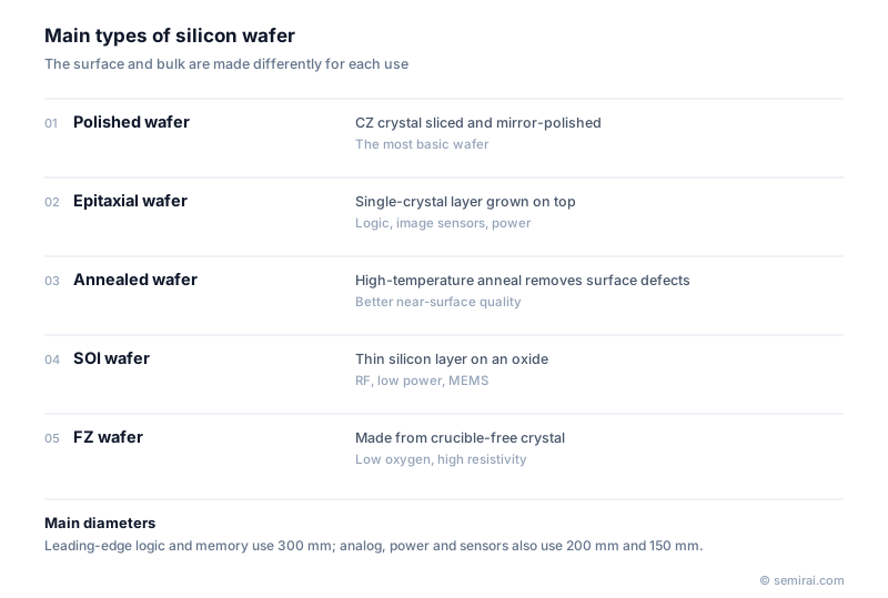
Polysilicon purified to around eleven nines (99.999999999%) is melted in a quartz crucible, and a seed crystal is slowly pulled and rotated to grow a cylindrical single-crystal ingot. This is the Czochralski (CZ) method, used for the great majority of wafers. A small share is grown by the float-zone (FZ) method, which avoids a crucible and gives very low oxygen content.
The ingot is ground to diameter, given a notch or flat to mark the crystal orientation, and sliced into wafers with a multi-wire saw. The wafers are then edge-rounded, lapped or ground, etched to remove damage, polished (usually on both sides for 300 mm) and cleaned, and every wafer is inspected for flatness and particles.
Sizes and specifications
Diameter has grown over the decades to today's 300 mm (12-inch) standard, used for nearly all leading-edge logic, DRAM and NAND flash. A larger wafer yields more chips per pass through each tool, which lowers cost per chip. Analog, power, sensor and MEMS fabs still run 200 mm and 150 mm lines. A move to 450 mm was studied but stalled because of the equipment investment it required.
Key specifications include thickness (775 µm for 300 mm), crystal orientation (mostly <100>), conductivity type and resistivity set by boron or phosphorus doping, oxygen and carbon content, flatness such as total thickness variation (TTV) and site flatness, surface roughness and the density of light point defects.
Types of wafer
Besides plain polished wafers, makers supply epitaxial wafers with a grown single-crystal surface layer, annealed wafers heat-treated to remove near-surface defects, and silicon-on-insulator (SOI) wafers with a thin silicon layer on buried oxide. Wafers made of other materials, such as silicon carbide or gallium arsenide, are sold separately as compound semiconductor substrates.
Japanese companies involved
- Shin-Etsu Chemical (through Shin-Etsu Handotai) and SUMCO are two of the main silicon wafer manufacturers, producing polished, epitaxial, annealed and SOI wafers in 200 mm and 300 mm.
- Hamai Industries makes lapping and polishing machines used in wafer production.
- Shin-Etsu Chemical · Silicon wafers, photoresists and photomask blanks
- SUMCO · Silicon wafers
- Hamai Industries · Lapping and polishing machines for wafers
FAQ
Is a silicon wafer the same as a semiconductor wafer?
Usually the two are used interchangeably, because most chips are made on silicon. Strictly, semiconductor wafer is the broader term and also covers silicon carbide, gallium nitride, gallium arsenide, indium phosphide and germanium substrates.
How many chips come from one wafer?
It depends on die size. A 300 mm wafer can hold thousands of small microcontroller or sensor dies but only a few dozen of the largest processors. Edge exclusion, scribe lines and yield losses reduce the number of good chips further.
Why do fabs care so much about wafer flatness?
Lithography prints within a depth of focus of well under a micrometre at advanced nodes. Any local thickness variation or warp moves part of the exposure field out of focus, so flatness specifications become stricter at each new node.
Comparisons
Related pages
Sources
Last updated: November 2, 2026