Orientation Flat / Notch
An orientation flat and a notch are marks on the edge of a wafer that show its crystal orientation. A round wafer looks the same from every angle, so a straight flat ground along the edge, or a small V-shaped notch, gives equipment a reference for detecting and aligning the wafer's rotation.
Also called: orientation flat, OF, wafer notch, primary flat, secondary flat
Diagram
Flats and notches by wafer size
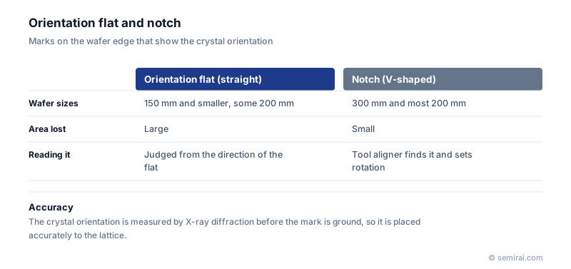
Smaller wafers, up to 150 mm, use a long primary flat to show the crystal direction. Under the SEMI standard, a shorter secondary flat placed at a defined angle to the primary flat indicates the conductivity type (p or n) and surface orientation. Notches are used on most 200 mm wafers and are standard on 300 mm wafers.
A flat removes a sizeable strip of the wafer. As diameters grew, that lost area mattered more, and the small notch replaced it.
How the mark is made and used
The flat or notch is ground at the same stage as the ingot's outer diameter. The crystal orientation is first measured by X-ray diffraction, so the mark is placed accurately relative to the lattice. If it were off, patterns would be rotated relative to the crystal, changing the shape of anisotropic etches and the way chips cleave.
In a process tool, an aligner in the equipment front-end module (EFEM) finds the notch optically and rotates the wafer to a fixed angle before it enters a process chamber. A badly shaped notch can cause detection failures and stop the tool. The notch is also a point of stress concentration, so its edge profile and polish affect chipping and particles.
Japanese companies involved
- Shin-Etsu Chemical and SUMCO grind notches and flats into their wafers to SEMI specifications as part of wafer shaping.
- Shin-Etsu Chemical · Silicon wafers, photoresists and photomask blanks
- SUMCO · Silicon wafers
- Okamoto Machine Tool Works · Wafer polishers and grinders
- Tokyo Seimitsu (ACCRETECH) · Wafer probers, dicing and grinding machines, metrology
FAQ
Why does crystal orientation matter at all?
Silicon is anisotropic. Interface state density, carrier mobility, wet etch rates and cleavage planes all depend on direction. MOS transistors are normally built on (100) silicon, and transistor channels are laid out along chosen directions within that plane.
Do laser marks replace the notch?
No. The laser-marked ID near the edge identifies the individual wafer for tracking, while the notch gives its orientation. Readers in the tool rely on the notch to find the ID in a known position.
Related pages
- Silicon Ingot
- Crystal Plane Orientation
- Miller Index
- EFEM (Equipment Front End Module)
- Silicon Wafer Manufacturing
- 200mm Wafer (8-inch Wafer)
- 300mm Wafer (12-inch Wafer)
- Cleavage
- Wire saws and wafer slicing equipment
- Okamoto Machine Tool Works ASM420M
- Tokyo Seimitsu (ACCRETECH) C-RW Series
- Asahi Diamond Industrial ECOMEP diamond wire
- Komatsu NTC MWM3050nQ
Sources
Last updated: November 13, 2026