Atomic Force Microscopy (AFM)
Atomic force microscopy (AFM) maps the three-dimensional shape of a surface by scanning a very sharp tip, mounted on a flexible cantilever, across it and detecting the tiny forces between tip and sample. It measures height with sub-nanometre resolution, works in air rather than vacuum, and handles insulators and conductors alike.
Also called: AFM, atomic force microscope, scanning probe microscopy
Diagram
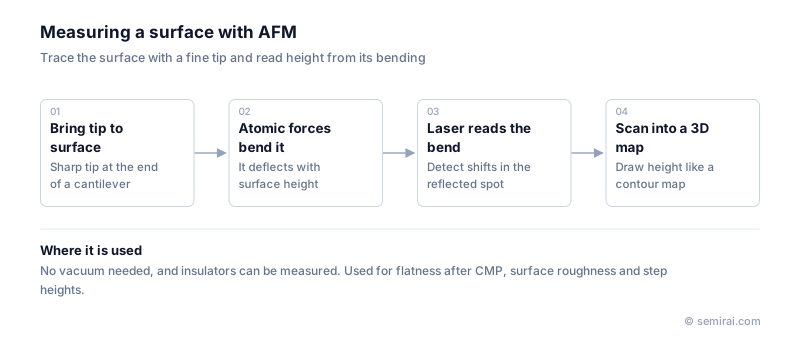
How AFM works
The tip, a few nanometres in radius at its apex, sits at the end of a microfabricated cantilever. As the tip meets the surface, attractive and repulsive forces bend the cantilever. A laser reflected off the back of the cantilever onto a position-sensitive photodetector reads this bending, an arrangement called an optical lever. A feedback loop moves the sample or tip up and down to keep the force constant, and the recorded movement becomes the height map.
In contact mode the tip drags across the surface. In tapping, or intermittent-contact, mode the cantilever oscillates near its resonance and touches the surface only briefly, which reduces damage and wear on soft or fragile samples. Non-contact modes sense the long-range forces without touching at all.
Uses in semiconductor manufacturing
Fabs use AFM to measure surface roughness after chemical mechanical planarization (CMP) and epitaxy, to check dishing and erosion of polished metal lines, and to measure step heights and the profiles of etched patterns. Automated AFMs that accept full wafers are used as reference tools to calibrate faster in-line methods.
Its weakness is speed and range. A scan covers an area of tens of micrometres at most and takes minutes, so AFM samples small sites rather than inspecting whole wafers. The tip shape also limits what it can see: it cannot reach the bottom of a trench narrower than the tip.
Japanese companies involved
- Hitachi High-Tech makes scanning probe microscopes, including AFMs, used for surface and materials research.
- Hitachi High-Tech · CD-SEM metrology, defect inspection and etch systems
FAQ
How is AFM different from SEM?
An SEM produces a projected image of a surface with very good lateral resolution but gives height only indirectly. AFM gives a true quantitative height map and needs no vacuum or conductive coating, but it is slower and covers a much smaller area.
What roughness values does AFM report?
The usual figures are Ra, the average absolute deviation from the mean height, and Rq or RMS, the root mean square deviation. For polished silicon wafers these are typically well below a nanometre, which only AFM-class instruments can measure reliably.
Related pages
Sources
Last updated: November 1, 2026