Scanning Electron Microscope (SEM)
A scanning electron microscope (SEM) forms an image by scanning a finely focused electron beam across a sample and detecting the electrons that come back from each point. Because electrons have a far shorter wavelength than light, an SEM resolves features of around a nanometre, well beyond the roughly 200 nm limit of an optical microscope.
Also called: SEM, scanning electron microscopy
Diagram
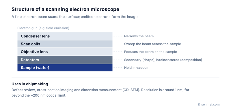
How an SEM works
An electron gun, usually a field emission source in modern instruments, produces the beam. Condenser and objective lenses, which are magnetic, focus it to a spot only a few nanometres wide, and scan coils sweep it across the sample in a raster. The column and sample sit in vacuum so that the electrons are not scattered by gas.
Detectors collect two main signals. Secondary electrons are low-energy electrons knocked out of the top few nanometres, and they show surface shape. Backscattered electrons are beam electrons reflected from deeper inside, and heavier elements reflect more of them, so they show composition contrast. The accelerating voltage, from below 1 kV to about 30 kV, sets how deep the beam reaches; low voltage is preferred for delicate resist patterns and to reduce charging.
How fabs use SEMs
A CD-SEM (critical dimension SEM) is a specialised low-voltage SEM that measures line widths and pattern edges on product wafers, automatically and at high throughput. A defect review SEM revisits the defect locations reported by an optical inspection tool and images each defect so it can be classified. FIB-SEM systems combine a focused ion beam with an SEM to cut and image cross-sections for failure analysis.
Electron beam inspection tools apply the same principle to find defects. Using voltage contrast, they reveal buried electrical faults such as opens and shorts that do not show up in an optical image.
Japanese companies involved
- Hitachi High-Tech makes CD-SEMs for in-line pattern measurement as well as defect review SEMs and FIB-SEM systems.
- JEOL makes scanning electron microscopes used in research and failure analysis laboratories.
- JEOL · Electron beam lithography systems, electron microscopes and surface analysis
- Hitachi High-Tech · CD-SEM metrology, defect inspection and etch systems
FAQ
Can an SEM look at a whole wafer without cutting it?
Yes. CD-SEMs and review SEMs take full wafers and image the surface directly. Cutting is needed only to see inside the structure, for example a cross-section of a trench, which is where FIB or cleaving comes in.
Why do insulating samples cause problems?
Electrons build up on surfaces that cannot conduct them away, distorting the image and shifting measurements. Fab tools reduce this by using low beam voltage and fast scanning; in laboratories samples are often coated with a thin metal or carbon film.
Comparisons
Related pages
Sources
Inspection and metrology terms
Last updated: November 2, 2026