Chemical Shift (XPS)
A chemical shift is a small change in a measured energy that depends on how an atom is bonded, not just which element it is. In semiconductor analysis the term usually refers to X-ray photoelectron spectroscopy (XPS), where shifts in core-level binding energy show the oxidation state of an element and what it is bonded to.
Also called: XPS chemical shift, binding energy shift
Diagram
Why the binding energy shifts
XPS shines X-rays on a sample and measures the kinetic energy of the emitted photoelectrons, from which the binding energy of each core electron is calculated. When an atom bonds to a more electronegative partner such as oxygen, valence electron density moves away from it. The core electrons then feel the nucleus more strongly, and their binding energy rises.
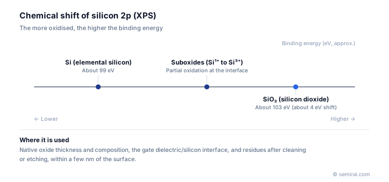
Silicon is the classic example. The Si 2p peak appears at about 99 eV for elemental silicon and about 103 eV for silicon dioxide, a shift of roughly 4 eV. Smaller peaks in between come from suboxides, silicon atoms bonded to one, two or three oxygen atoms, which are found at the Si/SiO₂ interface. Exact values depend on how charging is corrected.
Uses in chipmaking
Because XPS sees only the top few nanometres, chemical shifts are used to measure the thickness and composition of native oxides, to examine the interface between gate dielectric and silicon, to check bonding in high-k and nitrided films, and to identify residues after cleaning and etching. Sputtering with argon ions between measurements builds a depth profile, though the ion beam can itself alter some chemical states.
The same phrase is used in nuclear magnetic resonance (NMR) for a shift in nuclear resonance frequency. That is a different physical effect, and in semiconductor work the XPS meaning is the usual one.
Japanese companies involved
- ULVAC-PHI makes XPS instruments widely used for chemical-state analysis of semiconductor surfaces and thin films.
- Shimadzu, through its UK subsidiary Kratos Analytical, also supplies XPS systems.
FAQ
How can chemical shifts measure oxide thickness?
Photoelectrons from the substrate are weakened as they pass through the oxide on top. Comparing the intensity of the Si oxide peak with that of the elemental Si peak, and using the known electron attenuation length, gives the thickness of very thin oxides of a few nanometres.
Can a chemical shift be misread?
Yes. Insulating samples charge up under X-rays, which shifts all peaks together. Analysts correct this by referencing a known peak, often adventitious carbon, and must still allow for an uncertainty of a few tenths of an electronvolt when comparing with tables.
Comparisons
Related pages
- X-ray Absorption Near Edge Structure (XANES)
- Native Oxide
- Gate Oxide (Gate Dielectric)
- High-k Dielectric
- Secondary Ion Mass Spectrometry (SIMS)
- Failure Analysis (FA)
- X-ray Photoelectron Spectroscopy (XPS)
- Failure analysis equipment
- Hamamatsu Photonics Dual PHEMOS®-X C16506-01
- Hamamatsu Photonics iPHEMOS®-DDX C18040-11
- Hamamatsu Photonics iPHEMOS-MPX C10506-07-06
- Hamamatsu Photonics PHEMOS-X emission microscope C15765-01
Sources
Last updated: November 13, 2026