Microroughness
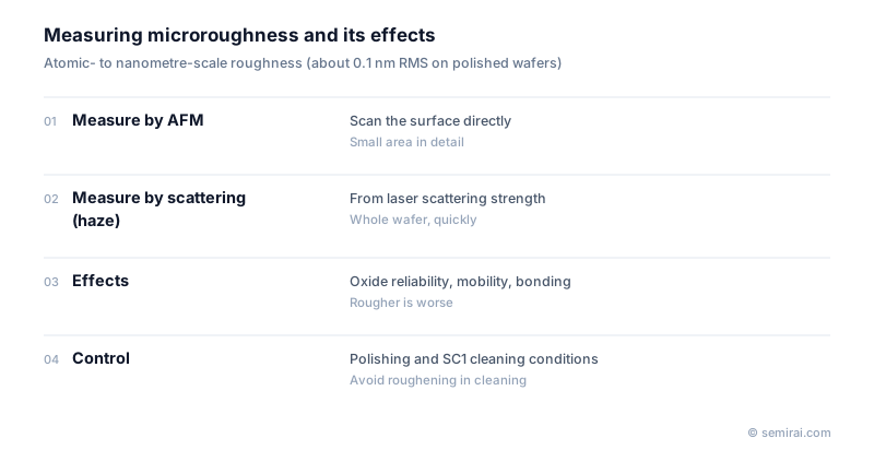
Microroughness is the fine unevenness of a surface, from the atomic scale up to a few nanometres in height. On a mirror-polished silicon wafer it is around 0.1 nm root mean square (RMS), about the size of one or two atoms. It affects gate oxide reliability, carrier mobility and wafer bonding, so wafer makers and fabs monitor it closely.
Also called: surface roughness, micro-roughness
Diagram
Where microroughness sits in wafer shape
Wafer surface shape is classified by the lateral size, or spatial wavelength, of the features. Long-wavelength features are warp and flatness across the whole wafer. Nanotopography covers height variation over a few millimetres. Microroughness is the finest level.
It is measured directly by scanning the surface with an atomic force microscope (AFM), or over the whole wafer by laser light scattering. A rough surface scatters a little light and makes the wafer look faintly hazy; the strength of this scattering is called haze and is measured together with particles by surface inspection tools. Roughness values are given as average roughness (Ra) or RMS roughness (Rq). They depend on the measured area and instrument, so comparisons need the same conditions.
Why it matters and how it is controlled
A rough silicon surface makes the thickness and insulating reliability of the gate oxide on top vary, and carriers in the transistor channel scatter off the interface, reducing mobility. In direct wafer bonding, rough surfaces bond weakly and leave voids.
Cleaning is a common cause of roughening. SC1 cleaning, with ammonia and hydrogen peroxide, slightly etches silicon, and a high ammonia ratio is known to roughen the surface, so fabs use diluted mixtures. Epitaxy, annealing and chemical mechanical polishing (CMP) conditions also affect microroughness.
Japanese companies involved
- SUMCO and other wafer makers finish polished wafers to sub-nanometre roughness and specify haze levels for advanced devices.
FAQ
How is microroughness different from nanotopography?
Both are surface height variations, but on different lateral scales. Nanotopography spans millimetres and affects lithography focus and CMP uniformity. Microroughness is far finer, at atomic to nanometre scale, and affects oxide and interface quality.
Why can AFM and haze measurements disagree?
They sample different spatial wavelengths. An AFM scan covers a small area at very high resolution, while haze integrates light scattered from a band of wavelengths across the whole wafer. Each is reliable for trends within its own conditions, but the numbers are not directly interchangeable.
Related pages
- Atomic Force Microscopy (AFM)
- SC1 Cleaning (APM)
- Wafer Flatness (TTV / SFQR / GBIR)
- Nanotopography
- Gate Oxide (Gate Dielectric)
- Wafer Bonding
- Carrier Mobility
- Line Edge Roughness (LER)
- Wafer polishing and edge grinding equipment
- DISCO DFP8141
- Fujikoshi Machinery MCP-200
- Fujikoshi Machinery SPM-23
- Komatsu NTC GCG300
Sources
Last updated: November 13, 2026