Dishing (CMP)
Dishing is a CMP defect in which the centre of a wide metal feature, such as a copper line or pad, is over-polished and sinks below the surrounding dielectric in a dish-like shape. It is most pronounced in copper CMP for damascene wiring, where it raises line resistance and leaves surface topography for the layers above.
Also called: metal dishing, copper dishing
Diagram
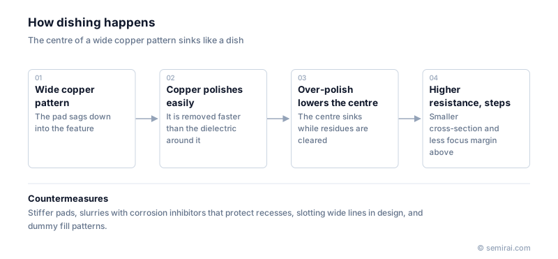
Why dishing happens
The polishing pad is slightly compliant. Over a wide metal line it bends down into the feature and keeps touching the metal even after the surrounding dielectric is exposed. Copper is also softer and more chemically reactive in the slurry than the dielectric, so it is removed faster.
Some over-polishing is always needed to clear metal residues across the whole wafer, and during that time the centre of wide lines keeps going down. The wider the feature, the more the pad can sag into it, so dishing grows with line width.
Effects and countermeasures
Thinner metal means a smaller cross-section and higher resistance, which adds RC delay and varies from line to line. The leftover depression also reduces flatness, eating into the depth-of-focus margin of the next lithography step, and the steps can accumulate over many wiring levels.
Dishing is reduced by tuning slurry selectivity between metal and dielectric, adding corrosion inhibitors such as benzotriazole (BTA) to protect recessed copper, using stiffer pads, controlling pressure and over-polish time, and adding design rules: wide lines are slotted and dummy fill patterns even out metal density. It is measured with atomic force microscopy or stylus profilers and tracked together with erosion as a key CMP quality indicator.
FAQ
Why is dishing a problem?
It reduces the cross-section of the line, so resistance rises, signals slow down and electromigration margin shrinks. The remaining topography also leaves the next layer less flat, which costs focus margin in lithography and can leave residues in later polishing steps.
What is the difference between dishing and erosion?
Dishing is a depression inside a single wide metal feature. Erosion is the thinning of a whole dense array of lines, where the dielectric between the lines is polished down along with the metal. Dishing reduces individual line thickness, while erosion lowers an entire region and adds to step height across wiring levels.
Can chip design help reduce dishing?
Yes. Design rules limit the maximum width of metal features, so very wide lines and pads are split with slots into narrower strips. Dummy metal fill is added to empty areas so that pattern density is more uniform, which makes the polish more even across the chip.
Related pages
Sources
Last updated: November 13, 2026