CD-SEM (Critical Dimension SEM)
A CD-SEM (critical dimension scanning electron microscope) is a scanning electron microscope built to measure the dimensions of circuit patterns on production wafers. It images lines, spaces and holes from above with a low-energy electron beam and automatically calculates their widths, so fabs can check after lithography and etch that patterns match the design.
Also called: critical dimension scanning electron microscope, measurement SEM
Diagram
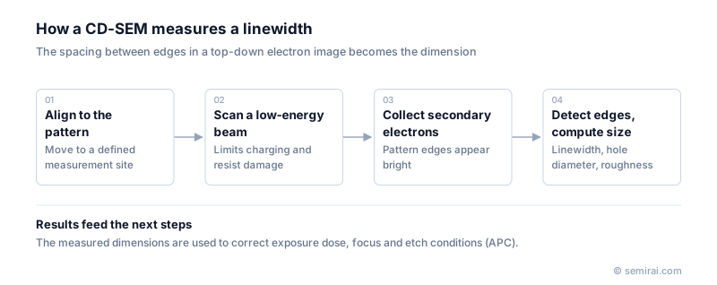
How a CD-SEM measures
The tool scans a finely focused electron beam across the pattern and collects the secondary electrons emitted from each point. Edges and sloped sidewalls emit more secondary electrons than flat areas, so they appear as bright lines in the signal profile. Software finds the edge positions in that profile and reports the distance between them as the critical dimension (CD).
Production CD-SEMs use low beam energies, typically around a kilovolt or less, to limit charging of insulating films and damage to photoresist. Some resists still shrink slightly under the beam, which has to be accounted for. Besides linewidth and space, the tools measure hole diameters, line-end positions and line edge and line width roughness (LER and LWR), which become a significant share of the total CD budget as features shrink.
Role in process control
A CD-SEM typically measures a sample of sites on selected wafers after develop, when the resist pattern can still be reworked, and again after etch, when the final dimension is set. The results go to advanced process control (APC) systems, which adjust exposure dose and focus on the scanner or etch time and conditions for following lots. This feedback loop keeps dimensions inside narrow windows across wafers and over time.
Because the measurement is a top-down image, a CD-SEM sees sidewall angle and depth only indirectly. Fabs therefore combine it with optical CD (scatterometry), which is faster and senses three-dimensional profiles, and with cross-sectional analysis for calibration.
Japanese companies involved
- Hitachi High-Tech makes CD-SEMs used for in-line pattern measurement in logic and memory fabs, along with defect review SEMs.
- Holon makes CD-SEMs for measuring patterns on photomasks.
- Holon · Photomask defect review, repair and CD-SEM metrology
- Hitachi High-Tech · CD-SEM metrology, defect inspection and etch systems
FAQ
What is the difference between a CD-SEM and an ordinary SEM?
An ordinary SEM is a general imaging instrument for laboratories. A CD-SEM is an automated production tool: it loads wafers from a FOUP, navigates to programmed sites, focuses and measures without an operator, and is tuned for repeatability so that the same feature gives the same number on every tool in a fab.
How does a CD-SEM compare with optical CD metrology?
Optical CD (scatterometry) fits the diffraction from periodic test structures to a model and returns average dimensions and profile shape quickly, without touching resist. A CD-SEM measures individual features, including irregular device patterns, and shows roughness directly, but is slower. The two are used together.
What is a design-based or contour CD-SEM measurement?
Instead of measuring a single width, the software extracts the full outline of a pattern from the image and compares it with the design layout. This helps verify optical proximity correction and find weak points in complex two-dimensional patterns.
Comparisons
Related pages
Sources
Last updated: November 2, 2026