CMP (Chemical Mechanical Polishing)
CMP (chemical mechanical polishing) is a process that flattens the wafer surface to nanometre level by combining chemical attack from a slurry with mechanical abrasion from a polishing pad. It removes the steps left by earlier layers so that the next layer can be patterned and stacked, and it is essential for building multilayer interconnects.
Also called: chemical mechanical planarisation, chemical mechanical planarization
Diagram
How it works
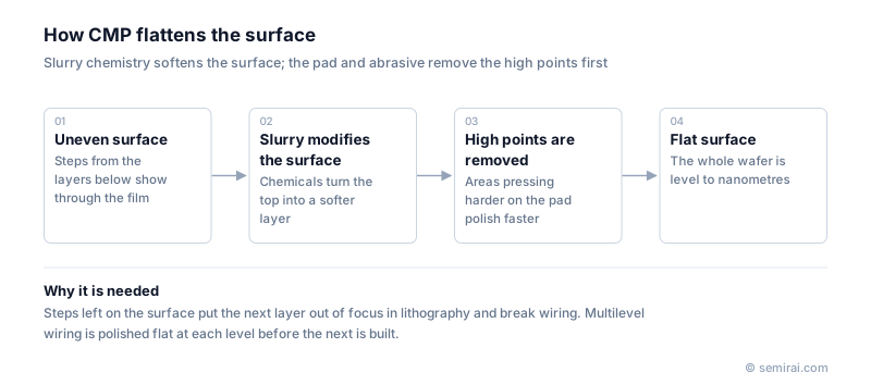
The wafer is held face-down in a polishing head and pressed against a pad mounted on a rotating table. Slurry, a liquid containing fine abrasive particles such as silica or ceria together with pH adjusters, oxidisers and surfactants, is fed onto the pad while the head and the table both rotate.
The chemicals convert the top of the film into a softer or more soluble layer, and the abrasive and pad wipe it away. Raised areas press harder against the pad than recessed areas, so they are removed faster, and the surface steadily becomes flat.
Where CMP is used
Typical steps include planarising the oxide that fills shallow trench isolation (STI), removing excess tungsten from contacts and vias, flattening the interlayer dielectric (ILD) between wiring levels, and removing excess copper and barrier metal in damascene interconnects. Copper cannot be patterned well by dry etching, so damascene wiring, and with it modern multilevel copper interconnects, depends on CMP. Replacement metal gate processes also use CMP to expose and trim the gate.
The main control parameters are removal rate, selectivity between materials, uniformity across the wafer, and pattern-dependent defects such as dishing of wide metal lines and erosion of dense arrays. Because these variations feed directly into device variation, slurry, pad and polishing conditions are optimised together for each step.
Japanese companies involved
- Ebara builds CMP systems used in front-end and interconnect polishing.
- Resonac and Fujimi Incorporated supply CMP slurries, and Nitta DuPont supplies polishing pads.
- Okamoto Machine Tool Works makes wafer polishers and grinders.
- Ebara · CMP systems, dry vacuum pumps and exhaust treatment
- Resonac · CMP slurries, packaging materials and SiC epitaxial wafers
- Fujimi Incorporated · CMP slurries and polishing materials
- Nitta DuPont · CMP and wafer polishing pads
- Okamoto Machine Tool Works · Wafer polishers and grinders
FAQ
Why is CMP needed?
In a multilayer chip the topography of each layer is copied into the layers above. Without planarisation the steps grow with every level, so parts of the surface fall outside the depth of focus of the lithography tool and thin films break over the edges. Polishing each level flat keeps patterning and wiring reliable.
What is a CMP slurry?
It is a water-based liquid containing abrasive particles and chemicals. Its composition is tuned to the material being removed: silica or ceria for oxide, and oxidisers plus corrosion inhibitors for copper or tungsten. The slurry largely sets the removal rate, selectivity and defect level of the step.
Is CMP the same as wafer polishing at the wafer maker?
They use similar equipment and abrasives, but the aims differ. Wafer makers polish bare silicon to a mirror finish before any device is built. Device-level CMP planarises patterned films such as oxide and copper and must stop at a precise depth without damaging the structures underneath.
Related pages
Sources
Last updated: November 2, 2026