Arsenic (As)
Arsenic (As), element 33 in group 15, is a donor that makes silicon n-type. Because it is heavy and diffuses slowly, it is the dopant of choice for the shallow, abrupt source/drain junctions of nMOS transistors. It is also a constituent element of compound semiconductors such as gallium arsenide (GaAs), InGaAs and AlGaAs.
Also called: n-type dopant, donor
Diagram
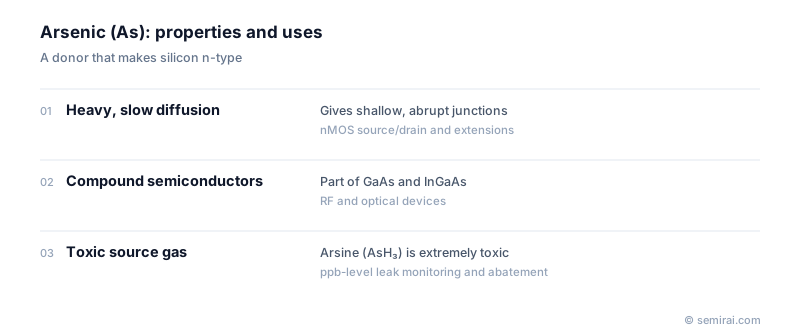
Why arsenic suits shallow junctions
With an atomic mass of about 75, arsenic is roughly 2.4 times heavier than phosphorus. At the same implant energy it stops closer to the surface, and it spreads little during annealing, so it gives shallow, abrupt junctions for nMOS source/drain regions and extensions.
Arsenic has high solid solubility in silicon and stays electrically active at high concentration, so it gives low-resistance regions. Its heavy ions amorphise the surface as they are implanted, which also limits channeling. It is used too for buried layers in bipolar transistors and for low-resistivity n-type silicon substrates.
Handling a very toxic material
Implanters use arsine (AsH₃) gas or solid arsenic as the source. Arsine is extremely toxic, with exposure limits at parts-per-billion levels, so it is supplied from sub-atmospheric cylinders where the gas is held on an adsorbent, and protected by leak detectors and exhaust abatement.
In compound semiconductor growth by metal-organic chemical vapour deposition (MOCVD), arsine or the less hazardous liquid source tertiarybutylarsine (TBAs) is used. Sludge and waste water from grinding and polishing GaAs wafers also contain arsenic and must be collected and treated under environmental regulations.
Japanese companies involved
- Sumitomo Electric Industries makes compound semiconductor substrates, including gallium arsenide (GaAs) wafers.
- Taiyo Nippon Sanso supplies specialty electronic gases and gas supply systems for hazardous process gases.
- Taiyo Nippon Sanso · Specialty gases, gas supply systems and MOCVD equipment
- Sumitomo Electric Industries (compound semiconductors) · SiC epitaxial wafers and GaAs and InP substrates
FAQ
Why not use arsenic everywhere instead of phosphorus?
Slow diffusion is an advantage only where a shallow junction is wanted. Deep wells would need very high implant energy with arsenic, and its heavy ions cause more crystal damage. Phosphorus is easier for deep or graded regions.
Why is GaAs used instead of silicon in some devices?
Electrons move faster in GaAs, and it has a direct band gap that emits light efficiently. This makes it suitable for radio-frequency amplifiers in phones and for LEDs and lasers, which silicon cannot do well.
Related pages
Sources
Ion implantation and thermal processing terms
Last updated: November 13, 2026