Donor and Acceptor
Donors and acceptors are the two kinds of impurity added to a semiconductor to set its conductivity type. Donors such as phosphorus and arsenic have one more valence electron than silicon and supply free electrons, making n-type material. Acceptors such as boron have one fewer and create holes, making p-type material.
Also called: donor impurity, acceptor impurity, n-type dopant, p-type dopant
Diagram
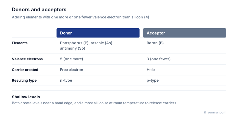
Why one extra or missing electron matters
Silicon has four valence electrons and bonds to four neighbours in the crystal. A donor atom from group 15, such as phosphorus, arsenic or antimony, has five. Four of them form bonds and the fifth is only weakly held, so at room temperature it is released into the conduction band as a free electron.
An acceptor from group 13, usually boron, has only three valence electrons. One bond is left incomplete, and a neighbouring electron easily moves in to fill it. The vacancy that moves through the crystal behaves as a positive carrier, a hole. In n-type silicon electrons are the majority carriers; in p-type silicon holes are.
Shallow and deep levels
In the band picture, a donor creates an energy level just below the conduction band edge, and an acceptor creates one just above the valence band edge. These shallow levels are only a few tens of millielectronvolts from the band edge, so almost all of them are ionised at room temperature and each dopant atom contributes one carrier.
Impurities such as gold, iron or other transition metals create deep levels near the middle of the band gap instead. They contribute few carriers but act as traps and recombination centres that increase leakage and shorten carrier lifetime, which is why metal contamination is controlled so strictly in fabs.
How dopants are introduced
In chip manufacturing, dopants are usually introduced by ion implantation, which controls the dose and depth precisely. Implantation damages the crystal and leaves most dopant atoms in non-lattice positions, so an activation anneal follows to repair the damage and move the atoms onto lattice sites, where they become electrically active.
Japanese companies involved
- Nissin Ion Equipment and Sumitomo Heavy Industries' ion implanter business make the ion implanters used to introduce donors and acceptors into wafers.
- Nissin Ion Equipment · Ion implanters
- Sumitomo Heavy Industries Material Solutions (formerly SMIT) · Ion implanters
FAQ
Which dopants are used in silicon?
Boron is the standard acceptor. Phosphorus and arsenic are the main donors, with antimony used for some heavily doped substrates. Arsenic diffuses slowly, which makes it useful for shallow, sharply defined junctions.
Can a region contain both donors and acceptors?
Yes. The type is decided by whichever is more concentrated, and the carriers from the other compensate part of them. Chipmakers use this to convert regions of a wafer from one type to the other by implanting a higher dose of the opposite dopant.
Related pages
Sources
Last updated: November 2, 2026