Doping
Doping is the addition of small, controlled amounts of impurities, called dopants, to a semiconductor to control its electrical properties. Adding phosphorus or arsenic makes silicon n-type, and adding boron makes it p-type. At concentrations from about 10¹⁴ to 10²⁰ atoms per cm³, the resistivity changes by many orders of magnitude.
Also called: impurity doping, dopant
Diagram
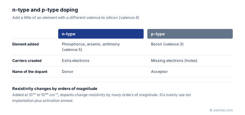
How dopants change silicon
Pure (intrinsic) silicon conducts very little at room temperature. A group-15 atom such as phosphorus has one more valence electron than silicon; on a lattice site, that extra electron is easily freed and carries current, so the atom is called a donor. A group-13 atom such as boron has one electron too few and creates a hole, so it is called an acceptor.
The amounts are tiny: roughly one dopant atom per few hundred to one per several hundred million silicon atoms. Higher doping lowers resistance but also reduces carrier mobility, and above the solid solubility limit extra atoms no longer become electrically active.
How doping is done
Thermal diffusion heats wafers in a furnace at around 900–1100 °C with a source such as POCl₃ or BBr₃; it is still used for solar cells. Ion implantation ionises the dopant, accelerates it and shoots it into the wafer, giving precise control of dose and depth, and is the mainstream method for integrated circuits. An activation anneal then repairs the crystal and moves dopants onto lattice sites.
In-situ doping adds dopant gas during epitaxy or CVD so that it is built into the film. Plasma doping is used to dope the sides of 3D structures such as fins, and whole wafers are made n-type or p-type by adding dopant to the melt during crystal pulling. A transistor combines many doped regions: wells, source/drain, channel doping for threshold voltage, and halo implants against short-channel effects.
Japanese companies involved
- Nissin Ion Equipment and Sumitomo Heavy Industries Material Solutions (formerly SMIT) make ion implanters, the main doping tools in chip fabs.
- Sumitomo Heavy Industries Material Solutions (formerly SMIT) · Ion implanters
- Nissin Ion Equipment · Ion implanters
FAQ
Why is an anneal needed after implantation?
Right after implantation the crystal is damaged and most dopant atoms sit between lattice sites, where they do not supply carriers. Annealing restores the crystal and lets the dopants take the place of silicon atoms, which is what makes them electrically active.
How is doping measured?
Sheet resistance is measured with a four-point probe, the depth profile of dopant atoms with secondary ion mass spectrometry (SIMS), and the carrier concentration and mobility with Hall-effect measurements.
Related pages
- Ion Implantation
- Dopant Activation
- Donor and Acceptor
- N-type and P-type Semiconductor
- Boron (B)
- Phosphorus (P)
- Arsenic (As)
- In-situ
- Diffusion furnaces
- Koyo Thermo Systems (JTEKT Thermo Systems) VF-5100
- Koyo Thermo Systems (JTEKT Thermo Systems) VF-5900
- Tokyo Electron (TEL) ALPHA-8SE™ i
- Tokyo Electron (TEL) EVAROS™
Sources
Last updated: November 13, 2026