EDA (Electronic Design Automation)
EDA (electronic design automation) is the family of software tools used to design integrated circuits. They take a chip from a hardware description of its behaviour, through logic synthesis, place and route, timing and power analysis and physical verification, to the GDSII layout file from which photomasks are made.
Also called: electronic design automation, chip design software
Diagram
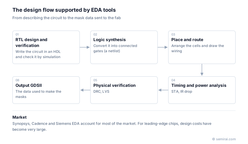
The main stages of the design flow
Designers first describe the circuit at the register-transfer level (RTL) in a hardware description language such as Verilog, SystemVerilog or VHDL, and check its behaviour with simulators, formal tools and emulators. Functional verification is usually the largest share of the engineering effort on a large chip.
Logic synthesis then turns the RTL into a gate-level netlist built from the foundry's standard cells. Place-and-route tools arrange millions or billions of cells on the die and draw the metal wiring between them. Static timing analysis (STA), power and IR-drop analysis and parasitic extraction check that the layout will run at the target speed and voltage.
Before tape-out the layout passes physical verification: design rule checking (DRC) confirms that every shape obeys the manufacturing rules, and layout versus schematic (LVS) confirms that the drawn layout matches the intended circuit. The result is written out as GDSII or OASIS data for mask making.
Why EDA matters for manufacturing
A modern processor holds tens of billions of transistors, so it cannot be drawn or checked by hand. EDA tools work from a process design kit (PDK) supplied by the foundry, which contains the design rules, device models and standard-cell libraries for a given process. Tools must be qualified for each new node, so foundries and EDA vendors develop flows together years before volume production.
At advanced nodes, process choices and design constraints affect each other so strongly that they are optimised together, an approach called design-technology co-optimisation (DTCO). Vendors have also added machine-learning features that search for better placement and parameter settings automatically, and are extending their tools to cover packages and multi-die systems as chiplets spread.
FAQ
Who are the main EDA vendors?
The market is dominated by three companies: Synopsys and Cadence Design Systems in the United States, and Siemens EDA, the former Mentor Graphics. Each sells tools across most of the flow, and their tools are certified against the PDKs of the major foundries.
Why is EDA described as a chokepoint?
Leading-edge chips cannot be designed without these tools, and supply is concentrated in a small number of US-headquartered vendors. For that reason EDA software for advanced nodes has been included in export controls alongside lithography equipment.
What is the difference between front-end and back-end design?
Front-end design covers architecture, RTL coding, verification and synthesis, where the circuit is defined logically. Back-end or physical design covers floorplanning, place and route, timing closure and signoff, where that logic becomes a manufacturable layout.
Related pages
Sources
Last updated: November 2, 2026