FEOL / BEOL (Front-End of Line / Back-End of Line)
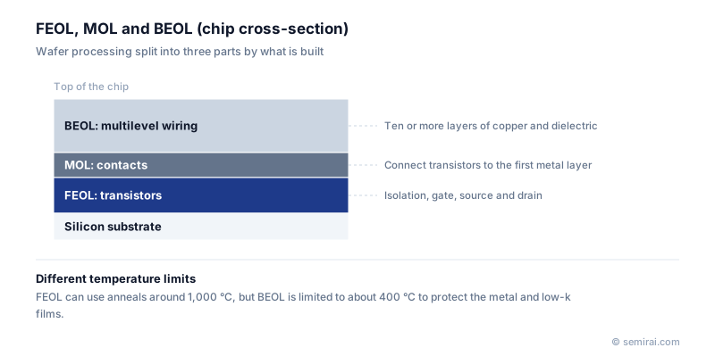
FEOL (front-end of line) and BEOL (back-end of line) divide wafer processing inside the fab into two parts. FEOL covers the steps that build the transistors in the silicon, and BEOL covers the multilevel metal wiring that connects them. Between them, the middle of line (MOL) forms the contacts that join transistors to the first metal layer.
Also called: FEOL, BEOL, MOL, middle of line
Diagram
What happens in each part
FEOL starts with device isolation by shallow trench isolation (STI), followed by well implants, gate dielectric formation by oxidation or high-k deposition, gate formation (in advanced logic, a replacement metal gate), source and drain implants and anneals, and silicide formation. At advanced nodes the main challenge is building three-dimensional FinFET or gate-all-around (GAA) transistors.
MOL forms small contacts, often filled with tungsten or cobalt, that reach the gate, source and drain. BEOL then builds the interconnect stack, from the finest lower metal layers to thick upper layers for power, often more than ten levels in all. Each level is made by depositing a low-k inter-layer dielectric, patterning it, etching trenches and vias, depositing barrier and seed layers, plating copper and polishing by CMP.
Different temperatures, different tools
FEOL can use high-temperature steps of around 1,000 °C for oxidation and dopant activation. Once metal and low-k films are on the wafer, BEOL processing is normally limited to about 400 °C to avoid damaging them. This temperature budget is one reason the two parts use different equipment: furnaces, implanters, epitaxy and ALD tools dominate FEOL, while copper PVD, electroplating, low-k CVD, dielectric etch and CMP dominate BEOL.
BEOL as a bottleneck
At the newest nodes the wiring has become as hard to scale as the transistors. As line pitch shrinks, copper's resistance rises, so alternative metals such as ruthenium and molybdenum are being introduced. Backside power delivery, which moves power wiring to the back of the wafer, is also changing where the boundary between transistors and wiring sits.
Japanese companies involved
- Tokyo Electron supplies deposition, etch and cleaning equipment used in both FEOL and BEOL, and Kokusai Electric makes batch furnaces for FEOL oxidation, deposition and ALD.
- Nissin Ion Equipment and Sumitomo Heavy Industries' ion implanter business make the implanters used for FEOL doping.
- Kokusai Electric · Batch deposition, diffusion and ALD equipment
- Nissin Ion Equipment · Ion implanters
- Sumitomo Heavy Industries Material Solutions (formerly SMIT) · Ion implanters
- Tokyo Electron (TEL) · Coat/develop, etch and deposition equipment
FAQ
Is BEOL the same as the back-end process?
No. BEOL is still wafer processing inside the fab. The back-end process, or back end, means packaging and test after the wafer is finished. Both terms use 'back end', which is why they are often confused.
Why is MOL treated separately?
At advanced nodes the contacts are so small and close to the gate that their resistance and the risk of shorts became a major problem of their own. Treating MOL as a separate module lets engineers focus on materials and processes specific to it.
Comparisons
Related pages
Sources
Last updated: November 2, 2026