Carrier Concentration
Carrier concentration is the number of mobile electrons (n) or holes (p) per unit volume of a semiconductor, usually given in cm⁻³. Together with mobility it sets resistivity. Pure silicon has only about 10¹⁰ cm⁻³ of each at room temperature, so devices are doped to between roughly 10¹⁵ and 10²⁰ cm⁻³.
Also called: carrier density, electron concentration, hole concentration
Diagram
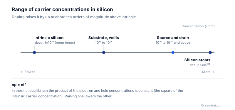
Intrinsic carriers and the mass-action law
In a pure (intrinsic) semiconductor, heat breaks bonds and creates electrons and holes in pairs, so n = p = ni, the intrinsic carrier concentration. For silicon at 300 K, ni is about 1×10¹⁰ cm⁻³, compared with about 5×10²² silicon atoms per cm³: fewer than one free carrier per trillion atoms, which is why pure silicon barely conducts. ni rises steeply with temperature and falls exponentially with band gap, so in SiC and GaN it is negligible at room temperature.
In thermal equilibrium the product np always equals ni², whether or not the material is doped. Adding donors raises n and lowers the hole concentration in the same proportion.
Setting the concentration by doping
With donors at concentration Nd fully ionised, n is approximately Nd; with acceptors, p is approximately Na. Substrates and wells are typically 10¹⁵–10¹⁷ cm⁻³, while source and drain regions, which need low resistance, reach 10¹⁹–10²⁰ cm⁻³ or more. The drift layers of power devices are kept lightly doped so the depletion region can spread and hold high voltage. At very high doping, mobility falls and not every dopant atom becomes electrically active.
Temperature dependence and measurement
At very low temperatures dopants do not ionise and carriers freeze out. Around room temperature the concentration is set by doping and is almost flat (the extrinsic range). At high temperatures intrinsic carriers exceed the dopant level and the device loses control; this sets the upper operating temperature, which is much higher for wide-bandgap SiC and GaN.
Hall-effect measurement gives the concentration of electrically active carriers, and C-V profiling gives its depth distribution from the spread of the depletion region. Secondary ion mass spectrometry (SIMS) measures dopant atoms chemically, including inactive ones.
FAQ
Is the dopant concentration measured by SIMS the same as the carrier concentration?
No. SIMS counts all dopant atoms, including those that sit off lattice sites or in clusters and contribute no carriers. Hall-effect or C-V measurements give the active carrier concentration; the ratio of the two is the activation rate, which shows how well an anneal worked.
Why do minority carriers matter if there are so few of them?
Many device currents are carried by minority carriers, including reverse leakage of junctions, bipolar transistor action and photocurrent in solar cells. Because np = ni², their concentration rises steeply with temperature, which is why junction leakage climbs quickly as a chip heats up.
What is a degenerate semiconductor?
One doped so heavily, roughly above 10¹⁹ cm⁻³ in silicon, that the Fermi level enters the conduction or valence band. It conducts almost like a metal and is used where low resistance or tunnelling is needed, such as ohmic contacts and tunnel junctions.
Related pages
Sources
Last updated: November 2, 2026