Carrier Mobility
Carrier mobility (µ) describes how easily electrons or holes move through a semiconductor under an electric field. It is the average drift velocity per unit field, given in cm²/V·s. Higher mobility means more current for the same voltage and faster transistors; in silicon, electrons are about three times more mobile than holes.
Also called: mobility, electron mobility, hole mobility
Diagram
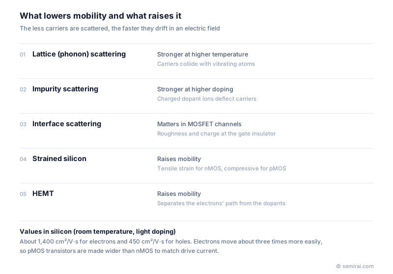
How mobility is defined
An electric field accelerates carriers, but they keep colliding with lattice vibrations, impurities and interfaces, so they settle at an average drift velocity proportional to the field: v = µE. Mobility grows with the average time between collisions and falls with the carrier's effective mass. Conductivity is the product of charge, carrier concentration and mobility, so mobility and doping together set a material's resistivity.
In lightly doped silicon at room temperature the electron mobility is about 1,400 cm²/V·s and the hole mobility about 450 cm²/V·s. For this reason pMOS transistors in CMOS circuits are drawn wider than nMOS transistors to deliver similar current. At very high fields the drift velocity stops rising and saturates, at around 10⁷ cm/s in silicon.
What lowers mobility
Lattice (phonon) scattering increases with temperature, so mobility in silicon falls as a chip heats up. Scattering by ionised dopants increases with doping, so heavily doped regions have lower mobility. In a MOSFET the carriers flow in a thin layer at the gate-insulator interface, where surface roughness and trapped charge scatter them further; channel mobility is therefore well below the bulk value.
Ways to raise mobility
Strained silicon changes the band structure to make carriers lighter: tensile strain helps electrons in nMOS, and compressive strain, often from SiGe source and drain regions, helps holes in pMOS. It entered volume production at the 90 nm generation. Germanium channels for pMOS and III-V compounds for nMOS have been studied for the same reason.
The high-electron-mobility transistor (HEMT) uses a heterojunction such as AlGaAs/GaAs or AlGaN/GaN to gather electrons in a two-dimensional electron gas away from the dopants, avoiding impurity scattering. Bulk GaAs reaches about 8,500 cm²/V·s for electrons. Bulk GaN is actually below silicon, at roughly 1,000 cm²/V·s; its high-mobility channel comes from the HEMT structure, around 2,000 cm²/V·s.
Japanese companies involved
- The HEMT was invented at Fujitsu Laboratories by Takashi Mimura around 1980 and is now used in satellite receivers, radar and base stations.
- Sumitomo Electric supplies GaAs and InP substrates used for high-mobility RF and optical compound-semiconductor devices.
- Sumitomo Electric Industries (compound semiconductors) · SiC epitaxial wafers and GaAs and InP substrates
FAQ
Why are holes slower than electrons in silicon?
Holes in silicon's valence band behave as if they were heavier than conduction electrons and scatter differently, so they gain less speed from the same field. The roughly threefold gap is a property of silicon's band structure, not of holes in general.
How is mobility measured?
Hall-effect measurement on a test sample gives the carrier concentration and, combined with resistivity, the Hall mobility. In finished transistors, an effective channel mobility is extracted from current-voltage and capacitance-voltage measurements.
Does higher mobility always mean a faster transistor?
Not proportionally. In very short channels carriers reach velocity saturation, and resistance in contacts and wiring also limits speed. Mobility still matters because it sets how quickly carriers approach that limit and the current at low voltage.
Related pages
Sources
Last updated: November 2, 2026