Dielectric Constant (k Value)
The dielectric constant, or relative permittivity, measures how strongly an insulator polarises and stores charge in an electric field, expressed as a ratio to vacuum. In the semiconductor industry it is called the k value. The capacitance of two electrodes separated by an insulator is proportional to k and inversely proportional to the insulator's thickness.
Also called: relative permittivity, permittivity, k
Diagram
Typical values
Vacuum has k = 1 and air almost exactly 1. Silicon dioxide (SiO₂) is about 3.9, silicon nitride about 7, aluminium oxide about 9 and hafnium oxide (HfO₂) about 20 to 25. Silicon itself is about 11.7 and GaAs about 12.9.
Low-k films used between interconnects, such as carbon-doped oxide (SiOC), are around 2.5 to 3.0, and porous versions go below 2.5. FR-4 circuit board material is around 4, while water is about 80.
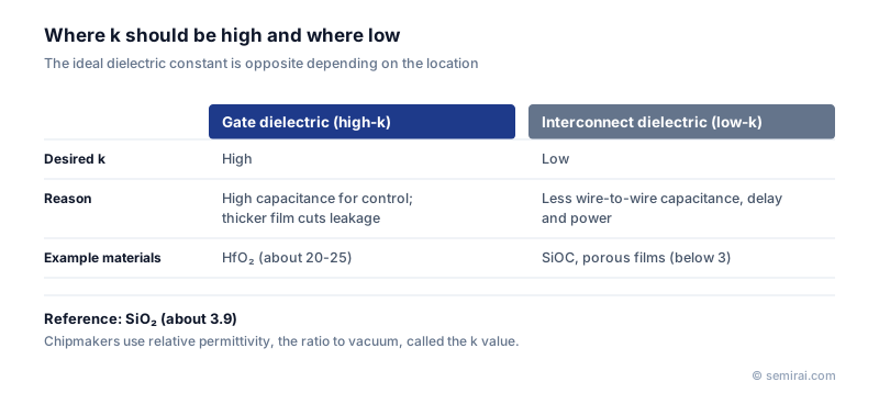
High-k in the gate, low-k between wires
A transistor gate dielectric needs high capacitance so the gate controls the channel strongly. Thinning SiO₂ raises capacitance, but below a few nanometres electrons tunnel through and leakage rises. High-k films such as HfO₂ give the same capacitance with a physically thicker layer. Their electrical thickness is quoted as equivalent oxide thickness (EOT), the SiO₂ thickness that would give the same capacitance.
Between interconnects the goal is the opposite. Capacitance between neighbouring wires slows signals and wastes power, so low-k films and even air gaps are used. High-speed circuit boards likewise use materials with low dielectric constant and low dissipation factor to cut loss and delay.
Japanese companies involved
- Tokyo Electron makes deposition systems, including ALD tools, used to form high-k gate films and low-k interlayer films.
- Tokyo Electron (TEL) · Coat/develop, etch and deposition equipment
FAQ
Why is SiO₂ (k about 3.9) used as the reference?
Silicon dioxide was the standard gate and interlayer insulator for decades, so new materials are compared against it. High-k means well above 3.9 and low-k means below it, and EOT expresses any gate stack as an equivalent thickness of SiO₂.
Why are low-k films difficult to integrate?
Lowering k usually means adding carbon or pores, which makes the film mechanically weaker and more easily damaged by plasma etching, cleaning and CMP. Moisture absorbed into pores can also raise k again, so low-k processing needs careful sealing and gentle steps.
Related pages
Sources
Last updated: November 2, 2026