Deep Reactive Ion Etching (DRIE)
Deep reactive ion etching (DRIE) is a dry etching technique that cuts deep features with nearly vertical side walls into silicon and other materials, at aspect ratios (depth divided by width) of ten or more. It is used to make MEMS devices, through-silicon vias (TSVs) and deep trenches in power devices.
Also called: DRIE, Bosch process, deep silicon etching
Diagram
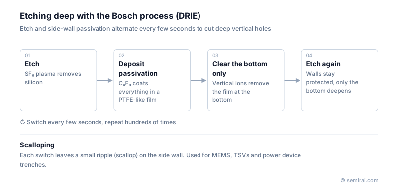
How the Bosch process works
The most widely used form of DRIE is the Bosch process, which alternates two short steps. In the etch step, an SF₆ plasma removes silicon. In the passivation step, a C₄F₈ plasma coats every surface with a thin fluorocarbon polymer similar to PTFE. When etching resumes, ions accelerated vertically toward the wafer strip the polymer from the bottom of the feature, while the side walls stay protected.
Switching every few seconds and repeating the cycle hundreds of times produces a deep hole or trench with vertical walls. Each cycle leaves a small ripple on the side wall, known as scalloping. Process tuning, such as shorter cycles, reduces the ripple when a smoother wall is needed.
Where DRIE is used
MEMS sensors such as accelerometers, gyroscopes and microphones rely on DRIE to form their moving silicon structures. In 3D packaging, DRIE etches the holes for TSVs, which are typically a few micrometres to about ten micrometres wide and tens of micrometres deep. Stacked memory such as HBM uses TSVs to carry signals and power vertically through each die, so via quality affects electrical performance.
Power MOSFETs and other power devices use deep trenches for their gate or field structures. The very deep, narrow holes in 3D NAND are cut through stacks of oxide and nitride layers rather than bulk silicon, using high-aspect-ratio dielectric etch, a related but different process.
Japanese companies involved
- SAMCO makes plasma etching systems, including deep silicon etching tools for MEMS and power devices, and Sumitomo Precision Products makes deep silicon etching equipment for MEMS.
- Tokyo Electron makes etch systems used for high-aspect-ratio etching in memory and logic.
- SAMCO · Plasma etching, CVD and plasma cleaning equipment
- Sumitomo Precision Products · MEMS and semiconductor manufacturing equipment (deep silicon etching)
- Tokyo Electron (TEL) · Coat/develop, etch and deposition equipment
FAQ
What is the difference between RIE and DRIE?
Reactive ion etching (RIE) uses a chemically reactive plasma plus ion bombardment and is used for most patterning in chipmaking, usually to depths below a few micrometres. DRIE is optimised to go much deeper, tens or hundreds of micrometres, while keeping the walls vertical.
Is there an alternative to the Bosch process?
Yes. Cryogenic etching cools the wafer far below 0 °C so that a passivating layer forms continuously while etching. It gives smoother walls without scalloping but needs tight temperature control.
Related pages
Sources
Last updated: November 13, 2026