Deposition
Deposition is the collective term for the processes that add thin films onto a wafer in semiconductor manufacturing. It forms the insulating, conducting and semiconducting layers that make up transistors, interconnects, barriers and protective coatings, and it is one of the most frequently repeated steps in a fab.
Also called: thin-film deposition, film formation
Diagram
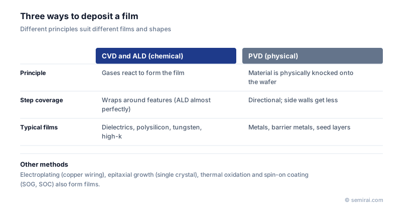
CVD, PVD and ALD
Chemical vapour deposition (CVD) forms a film through a chemical reaction of precursor gases on or near the wafer surface. It covers steps and trenches well, so it is used for dielectrics, polysilicon and tungsten fill. Plasma-enhanced CVD (PECVD) lets the reaction run at lower temperature.
Physical vapour deposition (PVD), mainly sputtering, knocks atoms off a solid target and lands them on the wafer. It gives pure metal films but is directional, so side walls receive less material; it is used for barrier metals and seed layers. Atomic layer deposition (ALD) supplies two precursors in turn so that each cycle adds roughly one atomic layer. It is slow but gives excellent thickness control and near-perfect coverage of 3D structures, which is why it is used for high-k gate dielectrics and very thin barriers.
Typical films and what they do
Common examples include polysilicon for gates and resistors, silicon oxide for insulation and trench isolation fill, silicon nitride for etch stops and spacers, hafnium oxide (HfO₂) as a high-k gate dielectric, tungsten for contact plugs, copper for interconnects, and tantalum or tantalum nitride as a copper barrier. Electroplating, epitaxial growth, thermal oxidation and spin-on coating are also counted as film formation.
What makes a good film
Engineers judge a deposition step by thickness uniformity across the wafer and from wafer to wafer, by step coverage in 3D features, and by film properties such as density, purity, stress and refractive index. At advanced nodes some films are only a few nanometres thick, so variations of a fraction of a nanometre affect transistor behaviour, reliability and yield.
Japanese companies involved
- Tokyo Electron makes CVD, ALD and other deposition systems, and Kokusai Electric makes batch furnaces for deposition and ALD that process many wafers at once.
- ULVAC and Canon ANELVA make sputtering (PVD) equipment.
- Kokusai Electric · Batch deposition, diffusion and ALD equipment
- ULVAC · Vacuum deposition (sputtering) equipment and vacuum pumps
- Canon ANELVA · Sputtering and vacuum deposition equipment
- Tokyo Electron (TEL) · Coat/develop, etch and deposition equipment
FAQ
When is ALD chosen over CVD?
ALD is chosen when a film must be extremely thin, uniform and conformal, for example inside deep trenches or around gate-all-around transistors. CVD is faster and cheaper, so it remains the choice for thicker films where perfect coverage is not needed.
What is the difference between deposition and epitaxy?
Epitaxy is a special kind of deposition in which the new film continues the single-crystal structure of the substrate. Most other deposited films are amorphous or polycrystalline.
Related pages
Sources
Last updated: November 2, 2026