Secondary Ion Mass Spectrometry (SIMS)
Secondary ion mass spectrometry (SIMS) is an analysis method that bombards a sample with a focused primary ion beam and measures the mass of the secondary ions knocked out of its surface. By sputtering steadily deeper, SIMS records how the concentration of each element changes with depth, making it the standard tool for measuring dopant profiles in semiconductors.
Also called: SIMS, dynamic SIMS, TOF-SIMS
Diagram
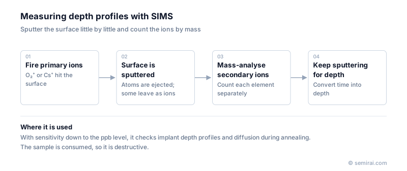
How SIMS works
A primary beam, typically oxygen ions (O₂⁺) or caesium ions (Cs⁺), strikes the sample and sputters away atoms from the surface. A small fraction of those atoms leave as ions. A mass spectrometer sorts the ions by mass-to-charge ratio and counts them for each element or isotope of interest. Oxygen enhances positive ion yield and suits elements such as boron, while caesium enhances negative ions and suits elements such as arsenic and phosphorus.
In dynamic SIMS the beam keeps sputtering a crater into the sample. Counting signals over time and measuring the final crater depth turns the time axis into a depth axis. Converting counts into concentrations requires reference samples of known composition, because the ion yield depends strongly on the matrix material.
What SIMS is used for
SIMS can detect dopants such as boron, phosphorus and arsenic at the parts-per-million to parts-per-billion level. Fabs and analysis laboratories use it to check ion implantation profiles, to see how far dopants diffuse during annealing, to confirm junction depth and to trace metal or light-element contamination in thin films.
Time-of-flight SIMS (TOF-SIMS) uses a pulsed, very gentle beam and analyses only the outermost layers. It is used to identify surface contamination, including organic residues, rather than to profile in depth.
Japanese companies involved
- ULVAC-PHI, a ULVAC group company, makes surface analysis instruments including TOF-SIMS and dynamic SIMS systems used in semiconductor laboratories.
- Japanese contract analysis laboratories such as Toray Research Center offer SIMS depth profiling for process development.
- ULVAC-PHI · Surface analysis instruments (XPS, TOF-SIMS)
- ULVAC · Vacuum deposition (sputtering) equipment and vacuum pumps
- Hitachi High-Tech · CD-SEM metrology, defect inspection and etch systems
FAQ
What are the limits of SIMS?
It is destructive, because the measured area is sputtered away. The analysed spot is usually tens of micrometres or more across, so very small features are hard to target, and the depth resolution degrades as the beam mixes atoms near the crater bottom. Accurate numbers also depend on matching reference standards.
When should I choose SIMS instead of EDX or XPS?
Choose SIMS when you need trace concentrations versus depth, such as a dopant profile. EDX in an electron microscope is better for the composition of a small spot at percent-level concentrations, and XPS is better for the chemical bonding state of the top few nanometres.
Comparisons
Related pages
Sources
Last updated: November 2, 2026