CCP (Capacitively Coupled Plasma)
CCP (capacitively coupled plasma) generates plasma by applying RF power between two parallel-plate electrodes so that the electric field between them ionises the gas. Its simple structure and the high ion energy it delivers make it well suited to etching oxide and nitride and to plasma-enhanced CVD (PECVD).
Also called: capacitively coupled plasma, parallel-plate plasma
Diagram
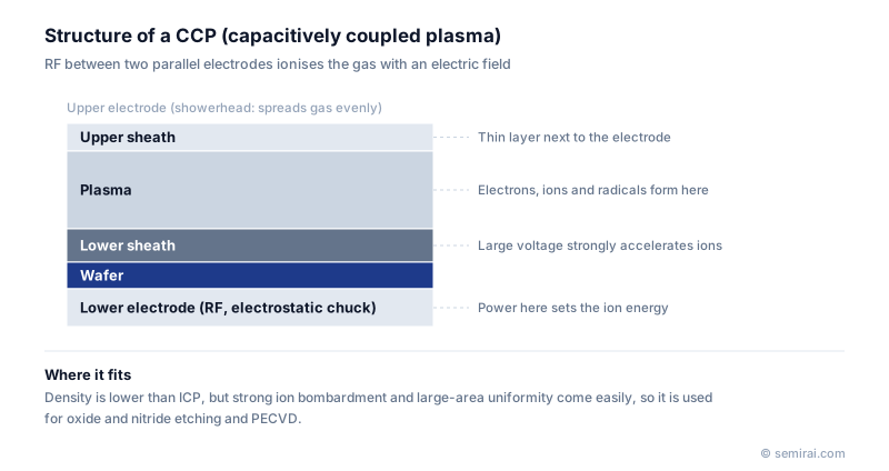
How CCP works
The wafer sits on the lower electrode, which also serves as the electrostatic chuck, and the upper electrode is usually a showerhead that distributes the gas evenly. RF power at frequencies such as 13.56, 27 or 60 MHz is applied to one or both electrodes. Thin sheaths form next to each electrode, and the strong field in the sheath above the wafer accelerates ions vertically into the surface, which produces anisotropic etching.
In a single-frequency CCP, raising the power increases plasma density and ion energy together. Dual-frequency systems add a high frequency that mainly controls density and a low frequency that mainly controls ion energy, giving partial independent control.
Strengths and limits
Plasma density in CCP is typically 10⁹–10¹⁰ cm⁻³, one to two orders of magnitude below ICP, and operating pressure is usually higher, from roughly ten to a few hundred mTorr. In return the hardware is simple and reliable, it produces uniform plasma over large wafers, and it easily delivers high bias voltage.
Where CCP is used
The main use is dielectric etching: contact holes and vias through silicon dioxide and silicon nitride with fluorocarbon gases, and the extremely deep holes of 3D NAND, where strong ion bombardment is needed. CCP is also the standard plasma source in PECVD chambers that deposit oxide and nitride films at low temperature.
Japanese companies involved
- Tokyo Electron (TEL) makes capacitively coupled etch systems used for dielectric etching in logic and memory production.
- SAMCO makes parallel-plate RIE and PECVD systems used in research and specialty device production.
- Tokyo Electron (TEL) · Coat/develop, etch and deposition equipment
- SAMCO · Plasma etching, CVD and plasma cleaning equipment
FAQ
Why is CCP used for oxide etching?
Silicon dioxide has strong bonds and is not etched fast enough by chemistry alone. It needs energetic ion bombardment to drive reactions with fluorocarbon species, and CCP readily provides the high bias voltage and ion energy this requires.
Why is the wafer electrode smaller than the grounded area?
In a parallel-plate system the smaller electrode develops a larger negative self-bias. Making the wafer electrode smaller than the grounded chamber walls concentrates ion bombardment on the wafer rather than on the chamber.
Comparisons
Related pages
Sources
Last updated: November 2, 2026