Etching
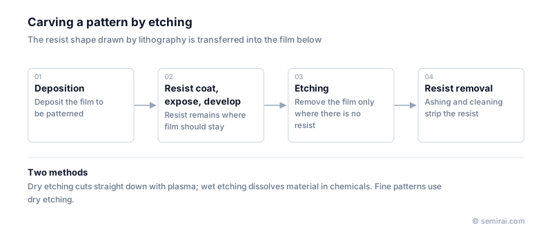
Etching is the front-end process that uses a resist pattern made by photolithography as a mask and selectively removes the film underneath. Lithography draws the pattern; etching carves it into real three-dimensional shapes. Together with deposition and lithography, it is one of the three basic processes of wafer fabrication.
Also called: etch, pattern etching
Diagram
Dry etching and wet etching
Dry etching uses a plasma in the gas phase. Ions arrive almost perpendicular to the wafer, so the etch can be anisotropic, cutting downward with vertical sidewalls. Wet etching dissolves material in chemicals and is isotropic, removing material equally in all directions and undercutting the mask.
For this reason fine patterns are defined almost entirely by dry etching today. Wet etching is still widely used for oxide removal, cleaning and selective removal of whole layers, where its high selectivity and low cost are useful.
How etch performance is measured
Four figures describe an etch. Etch rate is how fast material is removed. Uniformity is how evenly it is removed across the wafer. Selectivity is the ratio between the etch rate of the target film and that of the mask or underlying layer. Anisotropy compares vertical and lateral etching; reactive ion etching can make vertical etching dominate and produce straight sidewalls.
Where etching is used
Etching forms gate electrodes, contact and via holes, shallow trench isolation, the trenches and vias of copper damascene wiring, FinFET fins, the release of gate-all-around nanosheets and the high-aspect-ratio channel holes of 3D NAND. Each smaller node adds etch steps and tightens their precision, and atomic layer etching is now used in the most critical steps.
Japanese companies involved
- Tokyo Electron (TEL) and Hitachi High-Tech make dry etch systems, and SCREEN Holdings makes wet processing equipment used for wet etching and cleaning.
- Kanto Chemical supplies high-purity etchants for wet etching, and Daikin Industries supplies fluorine-based etching gases.
- Tokyo Electron (TEL) · Coat/develop, etch and deposition equipment
- Hitachi High-Tech · CD-SEM metrology, defect inspection and etch systems
- SCREEN Holdings · Wafer cleaning, coat/develop and inspection equipment
- Kanto Chemical · High-purity process chemicals for cleaning, etching and CMP
- Daikin Industries · Etching gases, fluoropolymers and fluoroelastomers
FAQ
What happens after etching?
The remaining resist is removed, usually by oxygen plasma ashing followed by wet cleaning to remove residues. The wafer then moves on to the next deposition or implantation step, and the cycle of deposition, lithography and etching is repeated for each layer.
Why is overetching used?
Film thickness and etch rate vary slightly across the wafer, so etching is continued for a short time after the film is cleared in most places. This makes sure no residue remains anywhere, and it is why high selectivity to the underlying layer matters.
Which companies make etch equipment?
The main suppliers of plasma etch systems are Lam Research, Tokyo Electron and Applied Materials, with Hitachi High-Tech and several smaller makers serving specific applications such as MEMS and compound semiconductors.
Comparisons
Related pages
Sources
Last updated: November 2, 2026