ICP (Inductively Coupled Plasma)
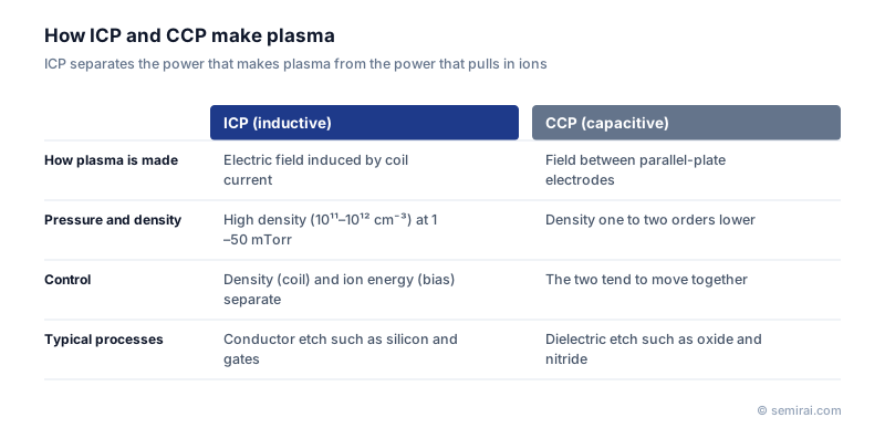
ICP (inductively coupled plasma) is a plasma generation method in which RF power is applied to a coil antenna, and the changing magnetic field induces an electric field that ionises the gas in the chamber. It sustains high-density plasma, typically 10¹¹–10¹² cm⁻³, at low pressures of about 1–50 mTorr.
Also called: inductively coupled plasma, ICP-RIE, TCP
Diagram
How ICP works
A coil sits above or around the chamber, separated from the plasma by a dielectric window. RF current in the coil, commonly at 13.56 MHz, creates a time-varying magnetic field, which induces an electric field inside the chamber that accelerates electrons and sustains the discharge.
A separate RF bias supply is connected to the electrode under the wafer. The coil power mainly sets plasma density and therefore etch rate, while the bias power sets the energy of ions hitting the wafer and therefore anisotropy, selectivity and damage. Being able to adjust these two independently is ICP's main advantage.
ICP compared with CCP
Compared with capacitively coupled plasma, ICP reaches densities one to two orders of magnitude higher, operates stably at lower pressure where ions travel straighter, and separates density from ion energy. The trade-offs are a more complex chamber and the design effort needed to keep a low-pressure, high-density plasma uniform across a 300 mm wafer.
Where ICP is used
ICP sources are widely used for etching conductors such as silicon, polysilicon gates and metals, for forming fins in advanced logic, and for compound semiconductors such as GaAs and InP. Deep silicon etching for MEMS and through-silicon vias, including the Bosch process, is also done in ICP chambers. In etch the method is often called ICP-RIE; Lam Research uses the name TCP (transformer coupled plasma) for its version.
Japanese companies involved
- Tokyo Electron (TEL) offers etch systems with inductively coupled plasma sources, and SAMCO makes ICP etchers used for compound semiconductors, MEMS and deep silicon etching.
- Tokyo Electron (TEL) · Coat/develop, etch and deposition equipment
- SAMCO · Plasma etching, CVD and plasma cleaning equipment
FAQ
What is the main benefit of ICP?
It keeps a dense plasma at low pressure while letting the bias power set ion energy separately. That combination gives fast etching without forcing high ion energy, so it is easier to achieve both a high etch rate and low damage.
When is CCP chosen over ICP?
For high-aspect-ratio etching of oxide and nitride, where strong, energetic ion bombardment is needed, capacitively coupled chambers are the usual choice. ICP is preferred where high density and low damage matter, such as silicon and metal etching. Some tools combine features of both.
Comparisons
Related pages
Sources
Last updated: November 2, 2026