Etch Selectivity
Etch selectivity is the ratio of the etch rate of the material to be removed to the etch rate of the material to be kept, such as the mask or the layer underneath. A higher value means the target film can be removed with little loss of the mask or underlayer, giving accurate dimensions and room for overetching.
Also called: selectivity, selectivity ratio
Diagram
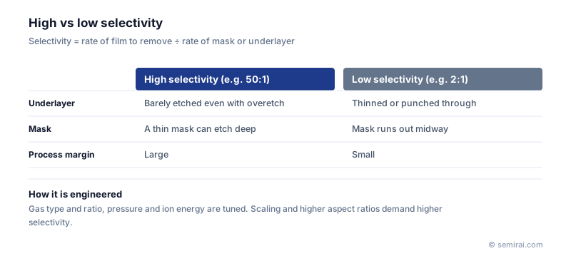
Why selectivity matters
Selectivity is usually quoted against two materials. Selectivity to the mask decides how deep an etch can go before the resist or hard mask is used up. Selectivity to the underlayer decides how much overetching is possible before the layer below is thinned or punched through.
Typical requirements are high. When polysilicon gates are etched, the thin gate oxide underneath must survive, so selectivities of many tens to one or more are needed. When contact holes are etched through oxide, the silicon at the bottom must not be damaged.
What controls selectivity
The main factors are gas chemistry, pressure, ion energy and temperature. Fluorocarbon gases for oxide etching form a polymer film that builds up on silicon and nitride surfaces, slowing their etching while the oxide continues to etch. Higher ion energy increases physical sputtering and generally lowers selectivity. Lower wafer temperature tends to increase polymer deposition and can raise selectivity. Process engineers combine these to reach the selectivity a step needs.
Selectivity at advanced nodes
In 3D NAND, channel holes pass through a stack of alternating oxide and nitride layers in one etch, so the chemistry must etch both at similar rates while staying highly selective to the mask. In gate-all-around transistors, sacrificial silicon germanium layers must be removed between silicon nanosheets with very high selectivity, using highly selective isotropic etches. Atomic layer etching is another way to gain selectivity.
Japanese companies involved
- Tokyo Electron (TEL) develops etch chambers and processes in which selectivity control is a central part of the design.
- Tokyo Electron (TEL) · Coat/develop, etch and deposition equipment
FAQ
What happens if selectivity is too low?
The mask or underlying film is etched along with the target. Pattern dimensions drift, the mask can be consumed before the etch is finished, or the etch can break through a thin stop layer and damage the device. These failures show up directly as yield loss.
How much selectivity is needed?
It depends on film thicknesses and their variation. As a rule of thumb ten to one or more is common, and a thin etch stop layer can require fifty to one or higher. Deep etches with thin masks need especially high selectivity to the mask.
Comparisons
Related pages
Sources
Last updated: November 2, 2026