PECVD (Plasma-Enhanced Chemical Vapour Deposition)
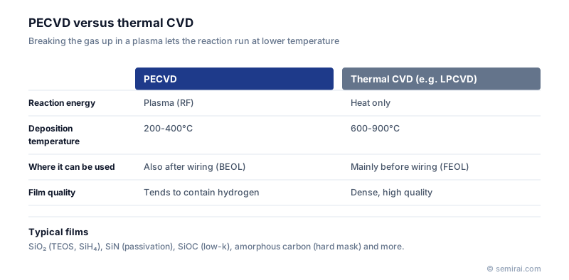
PECVD (plasma-enhanced chemical vapour deposition) is a CVD method in which an RF or microwave plasma excites and decomposes the precursor gases, so thin films can be deposited at roughly 200-400°C. Thermal CVD processes such as LPCVD typically need 600-900°C, so PECVD makes deposition possible after metal wiring and other temperature-sensitive layers are already on the wafer.
Also called: plasma CVD, plasma-enhanced CVD
Diagram
How PECVD works
In thermal CVD, heat alone has to supply the energy that breaks precursor molecules apart. In PECVD, electrons in a plasma collide with the gas and break it into reactive radicals and ions, which then react on the wafer surface at a much lower temperature. Most production PECVD chambers use a capacitively coupled plasma between a showerhead electrode and the heated wafer pedestal, often with two RF frequencies.
RF power, frequency, pressure, gas ratios and temperature give a wide window to tune film properties such as refractive index, density, hydrogen content and stress. Stress can be set from tensile to compressive, which is used deliberately in some layers and has to be controlled in thick stacks so the wafer does not bow.
Films and applications
Typical PECVD films are silicon oxide from silane or TEOS, silicon nitride from silane and ammonia, silicon oxynitride, carbon-doped oxide (SiCOH) low-k dielectrics, silicon carbonitride (SiCN) etch-stop and capping layers, amorphous silicon and amorphous carbon hard masks.
These films serve as interlayer dielectrics in multilevel wiring, as passivation layers that protect the finished chip, as etch hard masks and as antireflective layers for lithography. In 3D NAND, PECVD deposits the tall stacks of alternating silicon oxide and silicon nitride layers, where thickness uniformity across hundreds of layers and stress control are critical. The same technique is used widely for solar cells and flat-panel displays.
Limits and trade-offs
Low temperature comes at a cost. PECVD films contain more hydrogen and are less dense than thermally grown or LPCVD films, and step coverage in deep, narrow features is limited, so ALD or flowable CVD is used where conformal or void-free fill is required. Ion bombardment and charging can also damage sensitive layers, which is why plasma power and the plasma's position relative to the wafer are tuned carefully.
Japanese companies involved
- SAMCO makes plasma CVD systems, used mainly for compound semiconductor, optoelectronic and research applications.
- NGK Insulators makes ceramic heaters and susceptors that hold and heat the wafer inside deposition chambers.
- SAMCO · Plasma etching, CVD and plasma cleaning equipment
- NGK Corporation · Electrostatic chucks, ceramic heaters and susceptors
- Tokyo Electron (TEL) · Coat/develop, etch and deposition equipment
FAQ
What is the difference between PECVD and HDP-CVD?
HDP-CVD (high-density plasma CVD) uses an inductively coupled source to create a much denser plasma and applies bias to the wafer, so deposition and sputter etching happen at the same time. This lets it fill gaps between lines better than standard PECVD, and it was widely used for shallow trench isolation and pre-metal dielectric fill.
Why does PECVD silicon nitride contain hydrogen?
The precursors, silane and ammonia, contain hydrogen, and at low temperature not all Si-H and N-H bonds are broken. The hydrogen content changes the film's etch rate and stress, and in passivation layers it can diffuse to the silicon interface and passivate defects.
Is PECVD used in back-end or front-end processing?
Both, but its low temperature makes it essential in the back end, where copper and low-k dielectrics cannot tolerate high heat. In the front end it is used for hard masks and some liner and spacer films.
Comparisons
Related pages
Sources
Last updated: November 13, 2026