Charge-up
Charge-up is the build-up of electrical charge on insulators or on the wafer surface when charge delivered by a plasma, ion beam or electron beam has no path to escape. In semiconductor manufacturing it is a particular problem in plasma etching, ion implantation and scanning electron microscope (SEM) inspection. The stored charge creates electric fields that bend incoming particles or break down thin insulators.
Also called: charging, surface charging, charging damage
Diagram
Charging in plasma etching
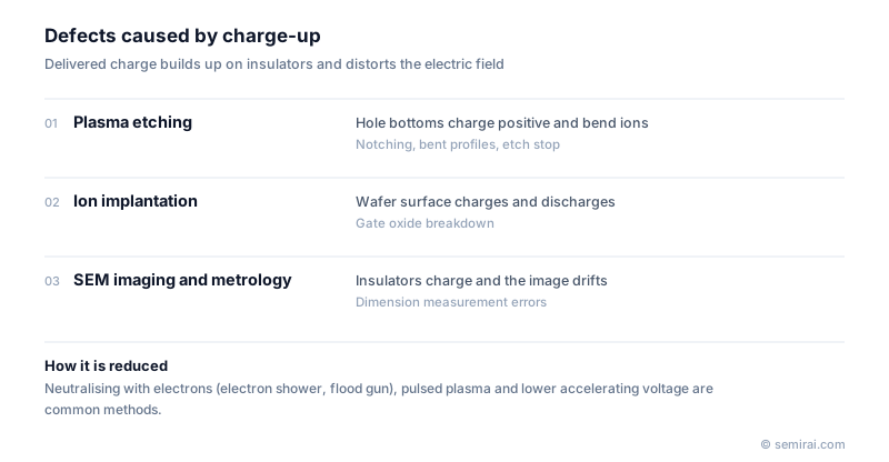
Electrons and ions arrive at the wafer differently. Electrons have random thermal directions, so many are caught on the upper sidewalls of narrow holes and trenches. Ions arrive almost vertically and reach the bottom. The top of the feature charges negatively and the bottom positively, an effect called electron shading.
The positive charge at the bottom repels and deflects later ions, which can stop the etch, distort the profile or cut sideways at the base of the feature, known as notching. Charge collected by wiring or gate electrodes can also flow through the gate oxide and degrade it; this plasma-induced damage is also called the antenna effect.
Charging in ion implantation and SEM
In ion implantation, a steady stream of positive ions charges resist and insulating films positively, and a discharge can destroy thin gate oxide. Implanters therefore include a plasma flood gun that supplies low-energy electrons to neutralise the wafer.
In SEM inspection, insulating samples charged by the electron beam appear abnormally bright or drift in the image, which causes errors in critical dimension (CD-SEM) measurements. Lower accelerating voltage, adjusted scanning and conductive coatings are used to reduce charging.
Japanese companies involved
- Nissin Ion Equipment and Sumitomo Heavy Industries Material Solutions make ion implanters, in which charge neutralisation of the wafer is a core part of the design.
- Hitachi High-Tech makes CD-SEM metrology systems, where managing sample charging is essential for accurate measurement.
- Nissin Ion Equipment · Ion implanters
- Sumitomo Heavy Industries Material Solutions (formerly SMIT) · Ion implanters
- Hitachi High-Tech · CD-SEM metrology, defect inspection and etch systems
- Tokyo Electron (TEL) · Coat/develop, etch and deposition equipment
FAQ
How is charging in plasma etching reduced?
Pulsing the plasma is a common method: in the off period electrons and negative ions can reach the bottom of features and neutralise the positive charge. Adjusting bias frequency and overetch conditions also helps, and antenna design rules limit how much charge can be collected onto a gate.
Why does charging get worse at advanced nodes?
Features are narrower and deeper, which strengthens electron shading, and advanced structures contain more insulating material where charge cannot escape. Gate dielectrics are also thinner, so they tolerate less stress from charging current.
Related pages
Sources
Last updated: November 2, 2026